AD9956/PCB Analog Devices Inc, AD9956/PCB Datasheet - Page 29
AD9956/PCB
Manufacturer Part Number
AD9956/PCB
Description
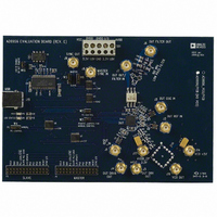
BOARD EVAL FOR AD9956
Manufacturer
Analog Devices Inc
Datasheet
1.AD9956YCPZ.pdf
(32 pages)
Specifications of AD9956/PCB
Module/board Type
Evaluation Board
For Use With/related Products
AD9956
Lead Free Status / RoHS Status
Contains lead / RoHS non-compliant


CFR1<3> = 0 (default). The automatic synchronization function
of the DDS core is disabled.
CFR1<3> = 1. The automatic synchronization function is on.
The device is slaved to an external reference and adjusts the
internal SYNC_CLK to match the external reference, which is
supplied on the SYNC_IN input.
CFR1<2> Software Manual Synchronization
Rather than relying on the part to automatically synchronize the
internal clocks, the user can program the part to advance the
internal SYNC_CLK one system clock cycle. This bit is self
clearing and can be set multiple times.
CFR1<2> = 0 (default). The SYNC_CLK stays in the current
timing relationship to SYSCLK.
CFR1<2> = 1. The SYNC_CLK advances the rising and falling
edges by one SYSCLK cycle. This bit is then self-cleared.
CFR1<1> Hardware Manual Synchronization
Similar to the software manual synchronization (CFR1<2>),
this function enables the user to advance the SYNC_CLK rising
edge by one system clock period. This bit enables the
PLL_LOCK/SYNC_IN pin as a digital input. Once enabled,
every rising edge on the SYNC_IN input advances the
SYNC_CLK by one SYSCLK period. While enabled, the
PLL_LOCK signal is not available on an external pin. However,
loop out-of-lock events trigger a flag in the control register
(CFR1<24>).
CFR1<1> = 0 (default). The hardware manual synchronization
function is disabled. Either the part is outputting the
PLL_LOCK (CFR1<3> = 0), or it is using the SYNC_IN to slave
the SYNC_CLK signal to an external reference provided on
SYNC_IN (CFR1<3> = 1).
CFR1<1> = 1. PLL_LOCK/SYNC_IN is set as a digital input.
Each subsequent rising edge on this pin advances the
SYNC_CLK rising edge by one SYSCLK period.
CFR1<0> High Speed Synchronization Enable Bit
This bit enables extra functionality in the auto synchronization
algorithm, which enables the device to synchronize high speed
clocks (SYNC_CLK > 62.5 MHz).
CFR1<0> = 0 (default). High speed synchronization is disabled.
CFR1<0> = 1. High speed synchronization is enabled.
Control Function Register 2 (CFR2)
This control register is comprised of five bytes, which must be
written during a write operation involving CFR2. With some
minor exceptions, the CFR2 primarily controls analog and tim-
ing functions on the AD9956.
Rev. A | Page 29 of 32
CFR2<39> DAC Power-Down Bit
This bit powers down the DAC portion of the AD9956 and puts
it into the lowest power dissipation state.
CFR2<39> = 0 (default). DAC is powered on and operating.
CFR2<39> = 1. DAC is powered down and the output is in a
high impedance state.
CFR2<38> to CFR2<34> Open
Unused locations. Write a Logic 0.
CFR2<33> Internal Band Gap Power-Down
To shut off all internal quiescent current , the band gap needs to
be powered down. This is normally not done because it takes a
long time (~10 ms) for the band gap to power up and settle to
its final value.
CFR2<33> = 0. Even when all other sections are powered down,
the band gap is powered up and is providing a regulated voltage.
CFR2<33> = 1. The band gap is powered down.
CFR2<32> Internal CML Driver DRV_RSET
To program the CML driver’s output current, a resistor
must be placed between the DRV_RSET pin and ground. This
bit enables an internal resistor to program the output current of
the driver.
CFR2<32> = 0 (default). The DRV_RSET pin is enabled,
and an external resistor must be attached to the CP_RSET pin
to program the output current.
CFR2<32> = 1. The CML current is programmed by the inter-
nal resistor and ignores the resistor on the DRV_REST pin.
CFR2<31:29> Clock Driver Rising Edge
These bits control the slew rate of the CML clock driver output’s
rising edge. When these bits are on, additional current is sent to
the output driver to increase the rising edge slew rate capability;
the contributions of each bit are cumulative. Table 6 describes
how the bits increase the current. Note that the additional cur-
rent is on only during the rising edge of the waveform for ap-
proximately 250 ps, but not on during the entire transition.
Table 6. CML Clock Driver Rising Edge Slew Rate
Control Bits and Associated Surge Current
CFR2<31> = 1
CFR2<30> = 1
CFR2<29> = 1
7.6 mA
3.8 mA
1.9 mA
AD9956
Related parts for AD9956/PCB
Image
Part Number
Description
Manufacturer
Datasheet
Request
R

Part Number:
Description:
400 Msps 14 Bit DDS EvBd. W/2450MHz VCO
Manufacturer:
Analog Devices Inc
Datasheet:
Part Number:
Description:
400 Msps 14 Bit DDS Eval Bd.
Manufacturer:
Analog Devices Inc
Datasheet:
Part Number:
Description:
BOARD EVAL 14BIT 1.8V 48LFCSP
Manufacturer:
Analog Devices Inc
Datasheet:


Part Number:
Description:
±1.7g Dual-Axis IMEMS Accelerometer Evaluation Board
Manufacturer:
Analog Devices Inc
Datasheet:
Part Number:
Description:
Inertial Sensor Evaluation System
Manufacturer:
Analog Devices Inc
Datasheet:
Part Number:
Description:
Manufacturer:
Analog Devices Inc
Datasheet:
Part Number:
Description:
Manufacturer:
Analog Devices Inc
Datasheet:
Part Number:
Description:
Manufacturer:
Analog Devices Inc
Datasheet:
Part Number:
Description:
Manufacturer:
Analog Devices Inc
Datasheet:
Part Number:
Description:
Manufacturer:
Analog Devices Inc
Datasheet:
Part Number:
Description:
Manufacturer:
Analog Devices Inc
Datasheet:
Part Number:
Description:
Manufacturer:
Analog Devices Inc
Datasheet: