DK-PCIE-2SGX90N Altera, DK-PCIE-2SGX90N Datasheet - Page 11
DK-PCIE-2SGX90N
Manufacturer Part Number
DK-PCIE-2SGX90N
Description
PCIE KIT W/S II GX EP2SGX90N
Manufacturer
Altera
Series
Stratix® IIr
Type
DSPr
Datasheet
1.DK-PCIE-2SGX90N.pdf
(36 pages)
Specifications of DK-PCIE-2SGX90N
Contents
Dev Board, Quartus®II Web Edition, Cables, Accessories, Reference Designs and Demos
For Use With/related Products
Stratix ll GX 2SGX90N
Lead Free Status / RoHS Status
Lead free / RoHS Compliant
Other names
544-1725


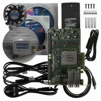
Figure 2–1. Stratix II GX PCI Express Development Board
Altera Corporation
March 2008
SFP Ports
Configuration Done
User DIP Switch
A and B
(J6, J7)
Ethernet RJ-45
External Clock Input
SMA Connector (J4)
Bank (S5)
Single Port
LED (D8)
Header
JTAG
(RJ1)
(J5)
QDRII SRAM (U6)
f
Flash Device (U3)
Stratix II GX Device (U10)
HSMC Interface A (J1)
Figure 2–1
Refer to the Stratix II GX EP2SGX90 PCI Express Development Board
Reference Manual (available on the PCI Express Development Kit,
Stratix II GX Edition CD-ROM) for information on the board’s
components.
Hardware Requirements
To run the pre-installed demo application design requires only a single
computer, Computer #1, with an x8 PCI Express slot to hold the
Stratix II GX PCI Express development board.
(D9 through D16)
User LEDs
Getting Started User Guide
shows the Stratix II GX PCI Express development board.
Edge Connector
PCI Express x8
High-Speed Mezzanine
Card Interfaces A & B
(J1 and J2)
PCI Express Development Kit, Stratix II GX Edition
SDRAM (U5, U8, U11, U13)
DDR2 32 x 16 Mbytes
Switches (S1 - S4)
User Push-Button
100 MHz
Crystal (X1)
155.25 MHz
Crystal (X4)
HSMC Interface B (J2)
DDR2 64 x 8 Mbytes
SDRAM (U2)
Transmit/Receive
Yellow LEDs
(D5 and D6)
Getting Started
Power Switch
Temperature
Sensor With
MAX II Device
Alarm (U7)
Power Supply
(SW1)
Input (J3)
(U4)
2–3
Related parts for DK-PCIE-2SGX90N
Image
Part Number
Description
Manufacturer
Datasheet
Request
R

Part Number:
Description:
Programmable Logic IC Development Tools FPGA Development Kit For 5AGTD7K3F40I3N
Manufacturer:
Altera Corporation
Datasheet:
Part Number:
Description:
Programmable Logic IC Development Tools FPGA Development Kit For 5SGXEA7N2F
Manufacturer:
Altera Corporation

Part Number:
Description:
PCI KIT W/CYCLONE II EP2C35N
Manufacturer:
Altera
Datasheet:

Part Number:
Description:
KIT, DEV, PCI EXPRESS, ECP2M
Manufacturer:
LATTICE SEMICONDUCTOR

Part Number:
Description:
Cyclone IV Tranceiver Development Kit
Manufacturer:
Altera
Datasheet:

Part Number:
Description:
KIT, DEV, CONNECTIVITY, SPARTAN-6
Manufacturer:
Xilinx Inc
Datasheet:

Part Number:
Description:
CYCLONE II STARTER KIT EP2C20N
Manufacturer:
Altera
Datasheet:

Part Number:
Description:
CPLD, EP610 Family, ECMOS Process, 300 Gates, 16 Macro Cells, 16 Reg., 16 User I/Os, 5V Supply, 35 Speed Grade, 24DIP
Manufacturer:
Altera Corporation
Datasheet:
Part Number:
Description:
CPLD, EP610 Family, ECMOS Process, 300 Gates, 16 Macro Cells, 16 Reg., 16 User I/Os, 5V Supply, 15 Speed Grade, 24DIP
Manufacturer:
Altera Corporation
Datasheet:
Part Number:
Description:
Manufacturer:
Altera Corporation
Datasheet:
Part Number:
Description:
CPLD, EP610 Family, ECMOS Process, 300 Gates, 16 Macro Cells, 16 Reg., 16 User I/Os, 5V Supply, 30 Speed Grade, 24DIP
Manufacturer:
Altera Corporation
Datasheet:
Part Number:
Description:
High-performance, low-power erasable programmable logic devices with 8 macrocells, 10ns
Manufacturer:
Altera Corporation
Datasheet: