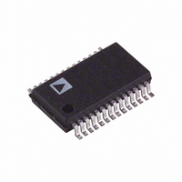
AD9225ARS Analog Devices Inc, AD9225ARS Datasheet

AD9225ARS
Specifications of AD9225ARS
Available stocks
Related parts for AD9225ARS
AD9225ARS Summary of contents
Page 1
FEATURES Monolithic 12-Bit, 25 MSPS ADC Low Power Dissipation: 280 mW Single 5 V Supply No Missing Codes Guaranteed Differential Nonlinearity Error: Complete On-Chip Sample-and-Hold Amplifier and Voltage Reference Signal-to-Noise and Distortion Ratio Spurious-Free Dynamic Range: –85 dB ...
Page 2
AD9225–SPECIFICATIONS (AVDD = 5 V, DRVDD = SPECIFICATIONS unless otherwise noted.) Parameter RESOLUTION MAX CONVERSION RATE INPUT REFERRED NOISE VREF = 1.0 V VREF = 2.0 V ACCURACY Integral Nonlinearity (INL) Differential Nonlinearity (DNL) No Missing ...
Page 3
V, DRVDD = SPECIFICATIONS otherwise noted.) Parameter SIGNAL-TO-NOISE AND DISTORTION RATIO (S/N+ 2.5 MHz INPUT MHz INPUT SIGNAL-TO-NOISE RATIO (SNR 2.5 MHz INPUT ...
Page 4
AD9225 Pin Name AVDD DRVDD AVSS AVDD REFCOM CLK Digital Outputs VINA, VINB VREF SENSE CAPB, CAPT Junction Temperature Storage Temperature Lead Temperature (10 sec) *Stresses above those listed under Absolute Maximum Ratings may cause permanent damage to the device. ...
Page 5
Pin Number 1 2 3– 15 TERMINOLOGY Integral Nonlinearity (INL) INL refers to the deviation of each individual code from a line drawn from negative ...
Page 6
AD9225–Typical Performance Characteristics (AVDD, DRVDD = MHz (50% Duty Cycle), unless otherwise noted.) S 1.00 0.75 0.50 0.25 0.00 –0.25 –0.50 –0.75 –1.00 0 511 1022 1533 2044 2555 Title TPC 1. Typical DNL 75 ...
Page 7
SFDR INT 2V REF –40 –35 –30 –25 –20 A (dB) IN TPC 7. SNR/SFDR vs. A (Input Amplitude 12.5 MHz, Input Span = 4 Differential ...
Page 8
AD9225 INTRODUCTION The AD9225 is a high performance, complete single-supply 12-bit ADC. The analog input range of the AD9225 is highly flexible, allowing for both single-ended or differential inputs of varying amplitudes that can be ac-coupled or dc-coupled. The AD9225 ...
Page 9
Due to the high degree of symmetry within the SHA topology, a significant improvement in distortion performance for differen- tial input signals with frequencies up to and beyond Nyquist can be realized. This inherent symmetry provides excellent cancella- tion of ...
Page 10
AD9225 REFERENCE OPERATION The AD9225 contains an on-board band gap reference that provides a pin strappable option to generate either output. With the addition of two external resistors, the user can generate reference voltages ...
Page 11
Input Input Connection Coupling Span (V) VINA* Single-Ended ¥ VREF ¥ VREF 2.0 – VREF Single-Ended ¥ VREF ¥ VREF 4 2 ¥ VREF 2.0 – ...
Page 12
AD9225 Differential modes of operation (ac-coupled or dc-coupled input) provide the best THD and SFDR performance over a wide fre- quency range. Differential operation should be considered for the most demanding spectral based applications (e.g., direct IF-to- digital conversion). See ...
Page 13
–V 2. 0.1 F Figure 8. Single-Ended AD9225 Op Amp Drive Circuit Op Amp with DC Level Shifting Figure 9 shows a dc-coupled level shifting circuit employing an op amp, A1, to ...
Page 14
AD9225 OP AMP SELECTION GUIDE Op amp selection for the AD9225 is highly dependent on the particular application. In general, the performance requirements of any given application can be characterized by either time domain or frequency domain parameters. In either ...
Page 15
Figure 13 shows the schematic of the suggested transformer circuit. The circuit uses a minicircuits RF transformer, model #T4-1T, which has an impedance ratio of 4 (turns ratio of 2). The sche- matic assumes that the signal source has a ...
Page 16
AD9225 REFERENCE CONFIGURATIONS The figures associated with this section on internal and external reference operation do not show recommended matching series resistors for VINA and VINB for the purpose of simplicity. Refer to the Driving the Analog Inputs and Introduction ...
Page 17
USING AN EXTERNAL REFERENCE Using an external reference may enhance the dc performance of the AD9225 by improving drift and accuracy. Figures 20 and 21 show examples of how to use an external reference with the ADC. Table III is ...
Page 18
AD9225 Table V. Out-of-Range Truth Table OTR MSB Analog Input Range Range 1 0 Underrange 1 1 Overrange MSB OTR MSB Figure 23. Overrange or Underrange Logic Digital Output Driver Considerations (DRVDD) The ...
Page 19
See Application Note AN-302 on using this technique in digital receivers. In direct IF down conversion applications, one exploits the inherent sampling process of an ADC in which an IF signal lying outside the baseband ...
Page 20
AD9225 100 95 SFDR 90 SINGLE-TONE (dBFS SFDR DUAL-TONE 70 (dBFS –15 –10 A (dBFS) IN Figure 29. IF Undersampling at 70 MHz ( 70.11 MHz, CLOCK = 25 MHz) 2 ...
Page 21
The digital activity on the AD9225 chip falls into two general categories: correction logic and output drivers. The internal correction logic draws relatively small surges of current, mainly during the clock transitions. The output drivers draw large current impulses while ...
Page 22
AD9225 U5 REF43 6 2 VOUT VIN 1 GND 1 C18 + C30 0.1 F R31 2 10V R25 2 820 2.49k 2 2 JP19 C29 ...
Page 23
Figure 36. Evaluation Board Component Side Layout (Not to Scale) Figure 37. Evaluation Board Ground Plane Layout (Not to Scale) Figure 38. Evaluation Board Component Side Silkscreen (Not to Scale) Rev. C Figure 39. Evaluation Board Solder Side Layout (Not ...
Page 24
... AD9225ARS −40°C to +85°C AD9225ARSRL −40°C to +85°C AD9225ARZ −40°C to +85°C AD9225ARZRL −40°C to +85°C AD9225ARSZ −40°C to +85°C AD9225ARSZRL −40°C to +85° RoHS Compliant Part. 18.10 (0.7126) 17.70 (0.6969 7.60 (0.2992) 7.40 (0.2913 ...
Page 25
REVISION HISTORY 1/11—REV REV. C Updated Outline Dimensions ....................................................... 24 Moved and Changes to Ordering Guide ..................................... 24 8/03—REV REV. B Renumbered TPCs and Figures ........................................ Universal Changes to Ordering Guide ............................................................ 4 Updated Outline Dimensions ...


