AD9281ARS Analog Devices Inc, AD9281ARS Datasheet
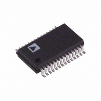
A/D Converter (A-D) IC

AD9281ARS

Manufacturer Part Number
AD9281ARS
Description
A/D Converter (A-D) IC
Manufacturer
Analog Devices Inc
Datasheet

Specifications of AD9281ARS

Peak Reflow Compatible (260 C)
No
Leaded Process Compatible
No
Package / Case
28-SOIC
Rohs Status
RoHS non-compliant
Number Of Bits
8
Sampling Rate (per Second)
28M
Data Interface
Parallel
Number Of Converters
2
Power Dissipation (max)
260mW
Voltage Supply Source
Analog and Digital
Operating Temperature
-40°C ~ 85°C
Mounting Type
Surface Mount
Lead Free Status / RoHS Status
Contains lead / RoHS non-compliant

Available stocks

Company
Part Number
Manufacturer
Quantity
Price
Part Number:
AD9281ARS
Manufacturer:
ADI/亚德诺
Quantity:
20 000
Part Number:
AD9281ARSZ
Manufacturer:
ADI
Quantity:
770
Part Number:
AD9281ARSZ
Manufacturer:
ADI/亚德诺
Quantity:
20 000
Part Number:
AD9281ARSZRL
Manufacturer:
ADI/亚德诺
Quantity:
20 000
REV. F
a
PRODUCT DESCRIPTION
The AD9281 is a complete dual channel, 28 MSPS, 8-bit
CMOS ADC. The AD9281 is optimized specifically for applica-
tions where close matching between two ADCs is required (e.g.,
I/Q channels in communications applications). The 28 MHz
sampling rate and wide input bandwidth will cover both narrow-
band and spread-spectrum channels. The AD9281 integrates
two 8-bit, 28 MSPS ADCs, two input buffer amplifiers, an internal
voltage reference and multiplexed digital output buffers.
Each ADC incorporates a simultaneous sampling sample-and-
hold amplifier at its input. The analog inputs are buffered; no
external input buffer op amp will be required in most applica-
tions. The ADCs are implemented using a multistage pipeline
architecture that offers accurate performance and guarantees no
missing codes. The outputs of the ADCs are ported to a multi-
plexed digital output buffer.
The AD9281 is manufactured on an advanced low cost CMOS
process, operates from a single supply from 2.7 V to 5.5 V, and
consumes 225 mW of power (on 3 V supply). The AD9281
input structure accepts either single-ended or differential signals,
providing excellent dynamic performance up to and beyond
14 MHz Nyquist input frequencies.
Information furnished by Analog Devices is believed to be accurate and
reliable. However, no responsibility is assumed by Analog Devices for its
use, nor for any infringements of patents or other rights of third parties
which may result from its use. No license is granted by implication or
otherwise under any patent or patent rights of Analog Devices.
FEATURES
Complete Dual Matching ADC
Low Power Dissipation: 225 mW (+3 V Supply)
Single Supply: 2.7 V to 5.5 V
Differential Nonlinearity Error: 0.1 LSB
On-Chip Analog Input Buffers
On-Chip Reference
Signal-to-Noise Ratio: 49.2 dB
Over Seven Effective Bits
Spurious-Free Dynamic Range: –65 dB
No Missing Codes Guaranteed
28-Lead SSOP
One Technology Way, P.O. Box 9106, Norwood, MA 02062-9106, U.S.A.
Tel: 781/329-4700
Fax:
PRODUCT HIGHLIGHTS
1. Dual 8-Bit, 28 MSPS ADC
2. Low Power
3. On-Chip Voltage Reference
4. On-chip analog input buffers eliminate the need for external
5. Single 8-Bit Digital Output Bus
6. Small Package
7. Product Family
REFSENSE
A pair of high performance 28 MSPS ADCs that are opti-
mized for spurious free dynamic performance are provided for
encoding of I and Q or diversity channel information.
Complete CMOS Dual ADC function consumes a low
225 mW on a single supply (on 3 V supply). The AD9281
operates on supply voltages from 2.7 V to 5.5 V.
The AD9281 includes an on-chip compensated bandgap
voltage reference pin programmable for 1 V or 2 V.
op amps in most applications.
The AD9281 ADC outputs are interleaved onto a single
output bus saving board space and digital pin count.
The AD9281 offers the complete integrated function in a
compact 28-lead SSOP package.
The AD9281 dual ADC is pin compatible with a dual 10-bit
ADC (AD9201).
QREFB
QREFT
781/461-3113
IREFB
IREFT
VREF
QINB
QINA
IINA
IINB
FUNCTIONAL BLOCK DIAGRAM
"Q" ADC
"I" ADC
REFERENCE
BUFFER
Resolution CMOS ADC
World Wide Web Site: http://www.analog.com
©1999-2011 Analog Devices, Inc. All rights reserved.
AVDD AVSS
Dual Channel 8-Bit
1V
REGISTER
REGISTER
ASYNCHRONOUS
Q
I
MULTIPLEXER
CLOCK
AD9281
DVDD
AD9281
OUTPUT
BUFFER
THREE-
STATE
DVSS
DATA
8 BITS
CHIP
SELECT
SLEEP
SELECT

Related parts for AD9281ARS

AD9281ARS Summary of contents

Page 1

FEATURES Complete Dual Matching ADC Low Power Dissipation: 225 mW (+3 V Supply) Single Supply: 2 5.5 V Differential Nonlinearity Error: 0.1 LSB On-Chip Analog Input Buffers On-Chip Reference Signal-to-Noise Ratio: 49.2 dB Over Seven Effective Bits ...

Page 2

AD9281–SPECIFICATIONS Parameter RESOLUTION CONVERSION RATE DC ACCURACY Differential Nonlinearity Integral Nonlinearity 1 Differential Nonlinearity (SE) 1 Integral Nonlinearity (SE) Zero-Scale Error, Offset Error Full-Scale Error, Gain Error Gain Match Offset Match ANALOG INPUT Input Voltage Range Input Capacitance Aperture Delay ...

Page 3

Parameter 1 DYNAMIC PERFORMANCE (SE) Signal-to-Noise and Distortion f = 3.58 MHz Signal-to-Noise f = 3.58 MHz Total Harmonic Distortion f = 3.58 MHz Spurious Free Dynamic Range f = 3.58 MHz DIGITAL INPUTS High Input Voltage Low Input Voltage ...

Page 4

AD9281 ABSOLUTE MAXIMUM RATINGS* With Respect Parameter to Min AVDD AVSS –0.3 DVDD DVSS –0.3 AVSS DVSS –0.3 AVDD DVDD –6.5 CLK AVSS –0.3 Digital Outputs DVSS –0.3 AINA, AINB AVSS –1.0 VREF AVSS –0.3 REFSENSE AVSS –0.3 REFT, REFB ...

Page 5

AVDD DRVDD DRVSS AVSS a. D0–D9 AVDD AVDD IN AVSS AVSS d. INA, INB OFFSET ERROR The first transition should occur at a level 1 LSB above “zero.” Offset is defined as the deviation of the actual first code transi- ...

Page 6

AD9281 –Typical Characteristic Curves (AVDD = +3 V, DVDD = + MHz (50% duty cycle input span from –0 +1 internal reference unless otherwise noted –1 ...

Page 7

CLOCK FREQUENCY – Hz Figure 9. THD vs. Clock Frequency 1.013 1.012 1.011 1.010 1.009 1.008 –40 – TEMPERATURE – C Figure 10. Voltage ...

Page 8

AD9281 10.0 FUND 0.0 –10.0 –20.0 –30.0 –40.0 –50.0 –60.0 3RD –70.0 2ND 9TH 8TH –80.0 –90.0 –100.0 –110.0 0.0E+0 2.0E+6 4.0E+6 6.0E+6 8.0E+6 10.0E+6 12.0E+6 14.0E+6 Figure 15a. Simultaneous Operation of I and Q Channels 10.0 FUND 0.0 –10.0 ...

Page 9

The AD9281 can accommodate a variety of input spans be- tween 1 V and 2 V. For spans of less than 1 V, expect a propor- tionate degradation in SNR. Use span will provide the best ...

Page 10

AD9281 REFERENCE AND REFERENCE BUFFER The reference and buffer circuitry on the AD9281 is configured for maximum convenience and flexibility. An illustration of the equivalent reference circuit is show in Figure 26. The user can select from five different reference ...

Page 11

ADC CORE 0.1 F IREFT IREFB 0.1 F VREF 1.0 F 0.1 F 10k REFSENSE INTERNAL CONTROL 10k LOGIC AVSS AD9281 Figure 26. Reference Buffer Equivalent Circuit and External Decoupling Recommendation For best results in ...

Page 12

AD9281 DIGITAL INPUTS AND OUTPUTS Each of the AD9281 digital control inputs, CHIP SELECT, CLOCK, SELECT and SLEEP are referenced to AVDD and AVSS. Switching thresholds will be AVDD/2. The format of the digital output is straight binary. A low ...

Page 13

At the receiver, the demodulation of a QAM signal back into its separate I and Q components is essentially the modulation process explain above but in the reverse order. A common and traditional implementation of a QAM demodulator is shown ...

Page 14

AD9281 REVISION HISTORY 1/11—Rev Rev. F Updated Format .................................................................. Universal Changes to Pin Configuration Diagram ........................................ 4 Changes to Pin Function Descriptions Table ................................ 4 Removed Evaluation Boards; Renumbered Sequentially ............................................................................ Changes to Ordering Guide ...

Page 15

... Temperature Range AD9281ARS −40°C to +85°C AD9281ARSRL −40°C to +85°C AD9281ARSZ −40°C to +85°C AD9281ARSZRL −40°C to +85° RoHS Compliant Part Shrink Small Outline. ©1999–2011 Analog Devices, Inc. All rights reserved. Trademarks and registered trademarks are the property of their respective owners. ...

Related keywords