BSS110 Fairchild Semiconductor, BSS110 Datasheet
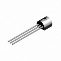
MOSFET P-CH 50V 170MA TO92

BSS110

Manufacturer Part Number
BSS110
Description
MOSFET P-CH 50V 170MA TO92
Manufacturer
Fairchild Semiconductor
Datasheet

Specifications of BSS110

Fet Type
MOSFET P-Channel, Metal Oxide
Fet Feature
Logic Level Gate
Rds On (max) @ Id, Vgs
10 Ohm @ 170mA, 10V
Drain To Source Voltage (vdss)
50V
Current - Continuous Drain (id) @ 25° C
170mA
Vgs(th) (max) @ Id
2V @ 1mA
Input Capacitance (ciss) @ Vds
40pF @ 25V
Power - Max
630mW
Mounting Type
Through Hole
Package / Case
TO-92-3 (Standard Body), TO-226
Lead Free Status / RoHS Status
Contains lead / RoHS non-compliant
Gate Charge (qg) @ Vgs
-

Available stocks

Company
Part Number
Manufacturer
Quantity
Price
Part Number:
BSS110
Manufacturer:
FSC
Quantity:
11 830
Part Number:
BSS110
Manufacturer:
NXPLIPS
Quantity:
5 510
Absolute Maximum Ratings
____________________________________________________________________________________________
© 2000 Fairchild Semiconductor Corporation
Symbol Parameter
V
V
V
I
P
T
T
THERMAL CHARACTERISTICS
R
D
J
L
DSS
DGR
GSS
D
,T
These P-Channel enhancement mode power field effect
transistors are produced using Fairchild's proprietary, high
cell density, DMOS technology. This very high density
process is designed to minimize on-state resistance, provide
rugged and reliable performance and fast switching. They
can be used, with a minimum of effort, in most applications
requiring up to 0.17A DC and can deliver pulsed currents up
to 0.68A. This product is particularly suited to low voltage
applications requiring a low current high side switch.
BSS84 / BSS110
P-Channel Enhancement Mode Field Effect Transistor
General Description
JA
STG
(TO-236AB)
BSS84
Drain-Source Voltage
Drain-Gate Voltage (R
Gate-Source Voltage - Continuous
Drain Current - Continuous @ T
Maximum Power Dissipation
Operating and Storage Temperature Range
Maximum lead temperature for soldering
purposes, 1/16" from case for 10 seconds
Thermal Resistance, Junction-to-Ambient
- Pulsed
GS
< 20 K )
@ T
A
T
= 25
A
A
= 30/35
= 25 ° C
T
A
o
C
= 25°C unless otherwise noted
o
C
Features
BSS110
BSS84
-0.13
-0.52
BSS84: -0.13A, -50V. R
BSS110: -0.17A, -50V. R
Voltage controlled p-channel small signal switch.
High density cell design for low R
High saturation current
0.36
350
-55 to 150
±20
300
-50
-50
G
.
DS(ON)
DS(ON)
= 10
BSS110
= 10
-0.17
-0.68
0.63
200
DS(ON)
@ V
S
D
BSS84 Rev. C2 / BSS110. Rev. A3
@ V
.
GS
GS
= -5V.
= -10V
May 2000
°C/W
Units
°C
°C
W
V
V
V
A

Related parts for BSS110

BSS110 Summary of contents

Page 1

... High density cell design for low R High saturation current BSS110 T = 25°C unless otherwise noted A BSS84 o = 30/35 C -0. -0. ° 0.36 A 350 May 2000 = -5V. DS(ON -10V DS(ON DS(ON BSS110 -50 -50 ±20 -0.17 -0.68 0.63 -55 to 150 300 200 °C/W BSS84 Rev BSS110. Rev. A3 Units °C °C ...

Page 2

... BSS110 2.2 10 BSS84 0.05 0.27 BSS110 0.05 0.29 BSS84 37 45 BSS110 37 40 All 16 25 All 5 12 All 12 All 50 All 10 All 25 BSS84 -0.13 BSS110 -0.17 BSS84 -0.52 BSS110 -0.68 BSS84 -0.95 -1.2 BSS110 -1 -1.2 BSS84 Rev BSS110. Rev. A3 Units V µA µA µ ...

Page 3

... Drain Current and Temperature 1.1 1.05 1 0.95 0.9 0. -25 Figure 6. Gate Threshold Variation = -3V -3 -4.5 -5 -0.2 -0.4 -0.6 -0 DRA IN CURRENT ( -10V 125°C J 25°C -55°C -0.2 -0.4 -0.6 -0 DRAIN CURRENT ( - 100 125 T , JUNCTION TEM PERATURE (°C) J with Temperature BSS84 Rev BSS110. Rev 150 ...

Page 4

... DUT V IN 10% Figure 12. Switching Waveforms 25°C -55°C 0.6 0.8 1 1.2 1.4 1 BODY DIODE FORWARD VOLTAGE (V) SD Variation with Source Current and Temperature V = -10V DS -20V -40V GATE CHARGE (nC off t t d(off) r 90% 90% 10% 10% 90% 50% 50% INVERTED PULSE W IDTH BSS84 Rev BSS110. Rev ...

Page 5

... SINGLE PULSE V = -10V DS 0.01 0.005 -0 Figure 14. Maximum Safe Operating Area 0.01 0 TIME (sec typical case-to-ambient thermal resistance V = -10V 25° DRAIN -SOURCE VOLTAGE ( ( C/W JA P(pk Duty Cycle 100 o C/W BSS84 Rev BSS110. Rev (t) 2 300 ...

Page 6

TO-92 Package Dimensions TO-92; TO-18 Reverse Lead Form (J35Z Option) (FS PKG Code 92, 94, 96) 1:1 Scale 1:1 on letter size paper Dimensions shown below are in: inches [millimeters] Part Weight per unit (gram): 0. Note: ...

Page 7

... TRADEMARKS The following are registered and unregistered trademarks Fairchild Semiconductor owns or is authorized to use and is not intended exhaustive list of all such trademarks. ACEx™ FAST Bottomless™ FASTr™ CoolFET™ FRFET™ CROSSVOLT™ GlobalOptoisolator™ GTO™ DenseTrench™ ...

Related keywords