BU4584B Rohm Semiconductor, BU4584B Datasheet
BU4584B
Specifications of BU4584B
Available stocks


Related parts for BU4584B


BU4584B Summary of contents
Page 1
... The BU4030B/BU4070B series can be used in digital comparators and parity circuits The BU4093B series are suitable as line receivers, waveform shaping and multi-vibrators, etc. The BU4584B series can be used in waveform shaping circuits for inputs with a slow rise time and fall time ●Lineup High Voltage CMOS Logic Logic Gate www ...
Page 2
... VDD VDD GND GND Input < > Technical Note Limit BU4081B BU4093B BU4069UB BU4584B -0 ±10 - -55 to 150 150 Limit BU4081B BU4093B BU4069UB BU4584B VDD UNIT mW/℃ VDD VDD GND GND Output < > 2009.06 - Rev.A Unit V mA ℃ ℃ V ℃ ...
Page 3
... BU4001B/F,BU4011B/F/FV,BU4030B/F,BU4070B/F, BU4081B/F/FV,BU4093B/F/FV,BU4069UB/F/FV,BU4584B/F/FV ●Electrical Characteristics(BU4001B)(Unless otherwise noted, VSS=0V, Ta=25℃, CL=50pF) Parameter Symbol Input “H” voltage VIH Input “L” voltage VIL Input “H” current Input “L” current Output “H” voltage VOH Output “L” voltage VOL Output “ ...
Page 4
... BU4001B/F,BU4011B/F/FV,BU4030B/F,BU4070B/F, BU4081B/F/FV,BU4093B/F/FV,BU4069UB/F/FV,BU4584B/F/FV ●Electrical Characteristics(BU4011B)(Unless otherwise noted, VSS=0V, Ta=25℃, CL=50pF) Parameter Symbol Input “H” voltage VIH Input “L” voltage VIL Input “H” current Input “L” current Output “H” voltage VOH Output “L” voltage VOL Output “ ...
Page 5
... BU4001B/F,BU4011B/F/FV,BU4030B/F,BU4070B/F, BU4081B/F/FV,BU4093B/F/FV,BU4069UB/F/FV,BU4584B/F/FV ●Electrical Characteristics(BU4030B/ BU4070B)(Unless otherwise noted, VSS=0V, Ta=25℃, CL=50pF) Parameter Symbol Input “H” voltage VIH Input “L” voltage VIL Input “H” current Input “L” current Output “H” voltage VOH Output “L” voltage VOL Output “ ...
Page 6
... BU4001B/F,BU4011B/F/FV,BU4030B/F,BU4070B/F, BU4081B/F/FV,BU4093B/F/FV,BU4069UB/F/FV,BU4584B/F/FV ●Electrical Characteristics(BU4081B)(Unless otherwise noted, VSS=0V, Ta=25℃, CL=50pF) Parameter Symbol Input “H” voltage VIH Input “L” voltage VIL Input “H” current Input “L” current Output “H” voltage VOH Output “L” voltage VOL Output “ ...
Page 7
... BU4001B/F,BU4011B/F/FV,BU4030B/F,BU4070B/F, BU4081B/F/FV,BU4093B/F/FV,BU4069UB/F/FV,BU4584B/F/FV ●Electrical Characteristics(BU4093B)(Unless otherwise noted, VSS=0V, Ta=25℃, CL=50pF) Parameter Symbol Input “H” voltage VIH Input “L” voltage VIL Input “H” current Input “L” current Output “H” voltage VOH Output “L” voltage VOL Output “ ...
Page 8
... BU4001B/F,BU4011B/F/FV,BU4030B/F,BU4070B/F, BU4081B/F/FV,BU4093B/F/FV,BU4069UB/F/FV,BU4584B/F/FV ●Electrical Characteristics(BU4069UB)(Unless otherwise noted, VSS=0V, Ta=25℃, CL=50pF) Parameter Symbol Input “H” voltage VIH Input “L” voltage VIL Input “H” current IIH Input “L” current Output “H” voltage VOH Output “L” voltage VOL Output “ ...
Page 9
... BU4001B/F,BU4011B/F/FV,BU4030B/F,BU4070B/F, BU4081B/F/FV,BU4093B/F/FV,BU4069UB/F/FV,BU4584B/F/FV ●Electrical Characteristics(BU4584B)(Unless otherwise noted, VSS=0V, Ta=25℃, CL=50pF) Parameter Symbol Input “H” voltage VIH Input “L” voltage VIL Input “H” current Input “L” current Output “H” voltage VOH Output “L” voltage VOL Output “ ...
Page 10
... BU4001B/F,BU4011B/F/FV,BU4030B/F,BU4070B/F, BU4081B/F/FV,BU4093B/F/FV,BU4069UB/F/FV,BU4584B/F/FV ●Switching Characteristics 20[ns 20[ 90% 50% Inpu 10% ①tPHL t ②tPLH 90% Output 50% 10% ③tTHL ④tTLH 20[ns 20[ 90% 50% 10% Inpu t ②tpHL ①tpLH 90% 50% Outpu 10% t ③tTLH ④tTHL www.rohm.com © 2009 ROHM Co., Ltd. All rights reserved. Description of Symbols (1) tPHL: Time up to 50% of rise time of input waveform ...
Page 11
... BU4001B/F,BU4011B/F/FV,BU4030B/F,BU4070B/F, BU4081B/F/FV,BU4093B/F/FV,BU4069UB/F/FV,BU4584B/F/FV ●Electrical Characteristics Curves(BU4001B) 6 [BU4001B/F] 5 85[℃] 25[℃] -40[℃ Input Voltage [V] Fig.1 Output voltage-Input voltage characteristics (VDD=5[V] / VSS=0[V]) 50 [BU4001B/F] VDD=15[V] -40[℃] 25[℃] 40 85[℃] VDD=10[V] 30 -40[℃] 25[℃] 85[℃] 20 VDD=5[V] -40[℃] 10 25[℃] 85[℃ Output Voltage [V] Fig.4 Output source current-voltage characteristics ...
Page 12
... BU4001B/F,BU4011B/F/FV,BU4030B/F,BU4070B/F, BU4081B/F/FV,BU4093B/F/FV,BU4069UB/F/FV,BU4584B/F/FV ●Electrical Characteristics Curves(BU4011B) 6 [BU4011B/F/FV] 5 85[℃] 25[℃] -40[℃ Input Voltage [V] Fig.10 Output voltage-Input voltage characteristics (VDD=5[V] / VSS=0[V]) 50 [BU4011B/F/FV] VDD=15[V] -40[℃] 40 25[℃] 85[℃] VDD=10[V] 30 -40[℃] 25[℃] 85[℃] 20 VDD=5[V] -40[℃] 10 25[℃] 85[℃ Output Voltage [V] Fig.13 Output source current-voltage characteristics ...
Page 13
... BU4001B/F,BU4011B/F/FV,BU4030B/F,BU4070B/F, BU4081B/F/FV,BU4093B/F/FV,BU4069UB/F/FV,BU4584B/F/FV ●Electrical Characteristics Curves(BU4030B / BU4070B) 6 [BU4030B/F] [BU4070B/F] 5 85[℃] 25[℃] -40[℃ Input Voltage [V] Fig.19 Output voltage-Input voltage characteristics (VDD=5[V] / VSS=0[V]) 50 [BU4030B/F] VDD=15[V] [BU4070B/F] -40[℃] 40 25[℃] 85[℃] VDD=10[V] 30 -40[℃] 25[℃] 85[℃] 20 VDD=5[V] -40[℃] 10 25[℃] 85[℃ Output Voltage [V] Fig.22 Output source current- ...
Page 14
... BU4001B/F,BU4011B/F/FV,BU4030B/F,BU4070B/F, BU4081B/F/FV,BU4093B/F/FV,BU4069UB/F/FV,BU4584B/F/FV ●Electrical Characteristics Curves(BU4081B) 6 [BU4081B/F/FV] 85[℃] 25[℃] -40[℃ Input Voltage [V] Fig.28 Output voltage-Input voltage characteristics (VDD=5[V] / VSS=0[V]) 50 [BU4081B/F/FV] VDD=15[V] -40[℃] 25[℃] 40 85[℃] VDD=10[V] -40[℃] 30 25[℃] 85[℃] 20 VDD=5[V] -40[℃] 10 25[℃] 85[℃ Output Voltage [V] Fig.31 Output source current-voltage characteristics ...
Page 15
... BU4001B/F,BU4011B/F/FV,BU4030B/F,BU4070B/F, BU4081B/F/FV,BU4093B/F/FV,BU4069UB/F/FV,BU4584B/F/FV ●Electrical Characteristics Curves(BU4093B) 6 [BU4093B/F/FV] 5 85[℃] 25[℃] -40[℃ Input Voltage [V] Fig.37 Output voltage-Input voltage characteristics (VDD=5[V] / VSS=0[V]) 50 [BU4093B/F/FV] VDD=15[V] -40[℃] 40 25[℃] 85[℃] VDD=10[V] -40[℃] 30 25[℃] 85[℃] 20 VDD=5[V] -40[℃] 25[℃] 85[℃ Output Voltage [V] Fig.40 Output source current-voltage characteristics ...
Page 16
... BU4001B/F,BU4011B/F/FV,BU4030B/F,BU4070B/F, BU4081B/F/FV,BU4093B/F/FV,BU4069UB/F/FV,BU4584B/F/FV ●Electrical Characteristics Curves(BU4069UB) 6 [BU4069UB/F/FV] 5 85[℃] 25[℃] -40[℃ Input Voltage [V] Fig.46 Output voltage-Input voltage characteristics (VDD=5[V] / VSS=0[V]) 50 [BU4069UB/F/FV] VDD=5[V] 40 -40[℃] VDD=10[V] 25[℃] -40[℃] 85[℃] 25[℃] 30 85[℃] 20 VDD=15[V] -40[℃] 25[℃] 85[℃ Output Voltage [V] Fig.49 Output source current-voltage characteristics ...
Page 17
... BU4001B/F,BU4011B/F/FV,BU4030B/F,BU4070B/F, BU4081B/F/FV,BU4093B/F/FV,BU4069UB/F/FV,BU4584B/F/FV ●Electrical Characteristics Curves(BU4584B) 6 [BU4584B/F/FV] 5 85[℃] 25[℃] 4 -40[℃ Input Voltage [V] Fig.55 Output voltage-Input voltage characteristics (VDD=5[V] / VSS=0[V]) 50 [BU4584B/F/FV] VDD=5[V] 40 -40[℃] VDD=10[V] 25[℃] -40[℃] 85[℃] 25[℃] 30 85[℃] 20 VDD=15[V] -40[℃] 25[℃] 85[℃ Output Voltage [V] Fig.58 Output source current-voltage characteristics ...
Page 18
... BU4001B/F,BU4011B/F/FV,BU4030B/F,BU4070B/F, BU4081B/F/FV,BU4093B/F/FV,BU4069UB/F/FV,BU4584B/F/FV ● Pinout Diagrams・Pin Description 1) BU4001B Series A1 VDD VSS 7 8 PIN No. PIN NAME I/O PIN FUNCTION INPUT1 INPUT1 OUTPUT1 OUTPUT2 INPUT2 INPUT2 7 VSS ― Power Supply(-) INPUT3 INPUT3 OUTPUT3 OUTPUT4 INPUT4 INPUT4 14 VDD ― Power Supply(+) TRUTH TABLE A B OUT ...
Page 19
... GND wiring pattern of any external components, either. 10. Unused input terminals Connect all unused input terminals to VDD or VSS in order to prevent excessive current or oscillation. Insertion of a resistor (100kΩ approx.) is also recommended www.rohm.com © 2009 ROHM Co., Ltd. All rights reserved. 8) BU4584B Series I1 VDD ...
Page 20
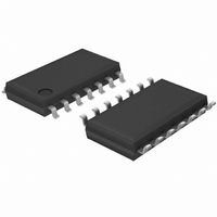
... BU4001B/F,BU4011B/F/FV,BU4030B/F,BU4070B/F, BU4081B/F/FV,BU4093B/F/FV,BU4069UB/F/FV,BU4584B/F/FV ●Ordering part number Part No. Part No. 4001B 4011B 4030B 4070B SOP14 8.7 ± 0.2 (MAX 9.05 include BURR 0.4 ± 0.1 1.27 0.1 SSOP-B14 5.0 ± 0 0.15 ± 0.1 0.1 0.65 0.22 ± 0.1 www.rohm.com © 2009 ROHM Co., Ltd. All rights reserved. ...
Page 21
... BU4001B/F,BU4011B/F/FV,BU4030B/F,BU4070B/F, BU4081B/F/FV,BU4093B/F/FV,BU4069UB/F/FV,BU4584B/F/FV DIP14 19.4±0 7.62 0°−15° 2.54 0.5±0.1 www.rohm.com © 2009 ROHM Co., Ltd. All rights reserved. <Tape and Reel information> Container Tube Quantity 1000pcs Direction of feed Direction of products is fixed in a container tube 0.3±0.1 (Unit : mm Technical Note ∗ ...
Page 22
No copying or reproduction of this document, in part or in whole, is permitted without the consent of ROHM Co.,Ltd. The content specified herein is subject to change for improvement without notice. The content specified herein is for the purpose ...