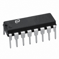
DAC0808LCN/NOPB National Semiconductor, DAC0808LCN/NOPB Datasheet

DAC0808LCN/NOPB
Specifications of DAC0808LCN/NOPB
*DAC0808LCN/NOPB
DAC0808
DAC0808LCN
Available stocks
Related parts for DAC0808LCN/NOPB
DAC0808LCN/NOPB Summary of contents
Page 1
... The DAC0808 will interface directly with popular TTL, DTL or CMOS logic levels, and is a direct replacement for the MC1508/MC1408. For higher speed applications, see DAC0800 data sheet. Block and Connection Diagrams © 2001 National Semiconductor Corporation Features n Relative accuracy: n Full scale current match: ± ...
Page 2
Block and Connection Diagrams Ordering Information ACCURACY OPERATING TEMPERATURE RANGE 8-bit 0˚ Note 1: Devices may be ordered by using either order number. www.national.com (Continued) Small-Outline Package DS005687-13 N PACKAGE (N16A) (Note 1) +75˚C DAC0808LCN 2 SO PACKAGE ...
Page 3
... Absolute Maximum Ratings If Military/Aerospace specified devices are required, please contact the National Semiconductor Sales Office/ Distributors for availability and specifications. Power Supply Voltage Digital Input Voltage, V5–V12 Applied Output Voltage Reference Current Reference Amplifier Inputs, V14, V15 Power Dissipation (Note 4) ESD Susceptibility (Note 5) ...
Page 4
Electrical Characteristics ( − /R14 = 2 mA, and all digital inputs at high logic level unless otherwise noted REF Symbol Parameter All Bits Low All Bits High Note 2: ...
Page 5
Typical Performance Characteristics noted (Continued) Output Current vs Output Voltage (Output Voltage Compliance) DS005687-17 Typical Power Supply Current DS005687-20 Unless otherwise specified: R14 = R15 = pF, pin ...
Page 6
www.national.com 6 ...
Page 7
Test Circuits V and I apply to inputs A1–A8 The resistor tied to pin temperature compensate the bias current and may not be necessary for all applications. and A = “1” ...
Page 8
Test Circuits (Continued) FIGURE 5. Transient Response and Settling Time (Note 8) FIGURE 6. Reference Current Slew Rate Measurement (Note 8) www.national.com DS005687-10 FIGURE 7. Positive V (Note 8) REF 8 DS005687-8 DS005687-9 ...
Page 9
Test Circuits (Continued) Application Hints REFERENCE AMPLIFIER DRIVE AND COMPENSATION The reference amplifier provides a voltage at pin 14 for converting the reference voltage to a current, and a turn-around circuit or current mirror for feeding the ladder. The reference ...
Page 10
Application Hints (Continued) advantage of this method. Compensation involves a capaci- tor pin 16, using the values of the previous EE paragraph. The negative reference voltage must be at least 4V above the V supply. Bipolar input ...
Page 11
Physical Dimensions inches (millimeters) unless otherwise noted Small Outline Package Order Number DAC0808LCM NS Package Number M16A Dual-In-Line Package Order Number DAC0808 NS Package Number N16A 11 www.national.com ...
Page 12
... NATIONAL’S PRODUCTS ARE NOT AUTHORIZED FOR USE AS CRITICAL COMPONENTS IN LIFE SUPPORT DEVICES OR SYSTEMS WITHOUT THE EXPRESS WRITTEN APPROVAL OF THE PRESIDENT AND GENERAL COUNSEL OF NATIONAL SEMICONDUCTOR CORPORATION. As used herein: 1. Life support devices or systems are devices or systems which, (a) are intended for surgical implant ...


