DS3668N/NOPB National Semiconductor, DS3668N/NOPB Datasheet

IC DVR QUAD FLT PROT PERF 16DIP

DS3668N/NOPB

Manufacturer Part Number
DS3668N/NOPB
Description
IC DVR QUAD FLT PROT PERF 16DIP
Manufacturer
National Semiconductor
Type
Driverr
Datasheet

Specifications of DS3668N/NOPB

Number Of Drivers/receivers
4/0
Voltage - Supply
3 V ~ 5.25 V
Mounting Type
Through Hole
Package / Case
16-DIP (0.300", 7.62mm)
Supply Voltage Min
3V
Supply Voltage Max
5V
No. Of Outputs
4
Output Voltage
70V
Output Current
600mA
Driver Case Style
DIP
Msl
MSL 1 - Unlimited
Device Type
Peripheral Driver
Rohs Compliant
Yes
Lead Free Status / RoHS Status
Lead free / RoHS Compliant
Protocol
-
Other names
*DS3668N
*DS3668N/NOPB
DS3668
DS3668N
DS3668N
© 2001 National Semiconductor Corporation
DS3668
Quad Fault Protected Peripheral Driver
General Description
The DS3668 quad peripheral driver is designed for those
applications where low operating power, high breakdown
voltage, high output current and low output ON voltage are
required. Unlike most peripheral drivers available, a unique
fault protected circuit is incorporated on each output. When
the load current exceeds 1.0A (approximately) on any output
for more than a built-in delay time, nominally 12 µs, that
output will be shut off by its protection circuitry with no effect
on other outputs. This condition will prevail until that protec-
tion circuitry is reset by toggling the corresponding input or
the enable pin low for at least 1.0 µs. This built-in delay is
provided to ensure that the protection circuitry is not trig-
gered by turn-on surge currents associated with certain
kinds of loads.
The DS3668’s inputs combine TTL compatibility with high
input impedance. In fact, its extreme low input current allows
it to be driven directly by a MOS device. The outputs are
capable of sinking 600 mA each and offer a 70V breakdown.
However, for inductive loads the output should be clamped
to 35V or less to avoid latch up during turn off (inductive
fly-back protection — refer AN-213). An on-chip clamp diode
capable of handling 800 mA is provided at each output for
this purpose. In addition, the DS3668 incorporates circuitry
that guarantees glitch-free power up or down operation and
a fail-safe feature which puts the output in a high impedance
state when the input is open.
The molded package is specifically constructed to allow
increased power dissipation over conventional packages.
The four ground pins are directly connected to the device
chip with a special copper lead frame. When the quad driver
is soldered into a PC board, the power rating of the device
improves significantly.
Connection Diagram
DS005225
See NS Package Number N16E
Dual-In-Line Package
Order Number DS3668N
Top View
Applications
n Relay drivers
n Solenoid drivers
n Hammer drivers
n Stepping motor drivers
n Triac drivers
n LED drivers
n High current, high voltage drivers
n Level translators
n Fiber optic LED drivers
Features
n Output fault protection
n High impedance TTL compatible inputs
n High output current — 600 mA per output
n No output latch-up at 35V
n Low output ON voltage (550 mV typ
n High breakdown voltage (70V)
n Open collector outputs
n Output clamp diodes for inductive fly-back protection
n NPN inputs for minimal input currents (1 µA typical)
n Low operating power
n Standard 5V power supply
n Power up/down protection
n Fail-safe operation
n 2W power package
n Pin-for-pin compatible with SN75437
DS005225-1
@
600 mA)
January 2001
www.national.com

Related parts for DS3668N/NOPB

DS3668N/NOPB Summary of contents

Page 1

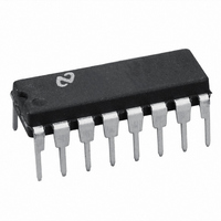
... The four ground pins are directly connected to the device chip with a special copper lead frame. When the quad driver is soldered into a PC board, the power rating of the device improves significantly. Connection Diagram © 2001 National Semiconductor Corporation Applications n Relay drivers n Solenoid drivers n Hammer drivers ...

Page 2

Truth Table High state L = Low state Z = High impedance state www.national.com OUT ...

Page 3

... Absolute Maximum Ratings If Military/Aerospace specified devices are required, please contact the National Semiconductor Sales Office/ Distributors for availability and specifications. Supply Voltage Input Voltage Output Voltage Continuous Power Dissipation @ 25˚C Free-Air (Note 5) Electrical Characteristics Symbol Parameter V Input High Voltage IH V Input Low Voltage ...

Page 4

AC Test Circuit Typical Application Protection Circuit Block Diagram www.national.com Switching Waveforms DS005225-2 4 DS005225-3 DS005225-4 DS005225-5 ...

Page 5

... NATIONAL’S PRODUCTS ARE NOT AUTHORIZED FOR USE AS CRITICAL COMPONENTS IN LIFE SUPPORT DEVICES OR SYSTEMS WITHOUT THE EXPRESS WRITTEN APPROVAL OF THE PRESIDENT AND GENERAL COUNSEL OF NATIONAL SEMICONDUCTOR CORPORATION. As used herein: 1. Life support devices or systems are devices or systems which, (a) are intended for surgical implant ...

Related keywords