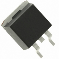
FDB045AN08A0 Fairchild Semiconductor, FDB045AN08A0 Datasheet

FDB045AN08A0
Specifications of FDB045AN08A0
Available stocks
Related parts for FDB045AN08A0
FDB045AN08A0 Summary of contents
Page 1
... This product has been designed to meet the extreme test conditions and environment demanded by the automotive industry. For a copy of the requirements, see AEC Q101 at: http://www.aecouncil.com/ Reliability data can be found at: http://www.fairchildsemi.com/products/discrete/reliability/index.html. All Fairchild Semiconductor products are manufactured, assembled and tested under ISO9000 and QS9000 quality systems ©2006 Fairchild Semiconductor Corporation FDB045AN08A0 Rev. A1 ® MOSFET Applications = 80A • ...
Page 2
... Drain-Source Diode Characteristics V Source to Drain Diode Voltage SD t Reverse Recovery Time rr Q Reverse Recovered Charge RR Notes: 1: Starting T = 25° 0.48mH 50A Pulse Width = 100s FDB045AN08A0 Rev. A1 Package Reel Size TO-263AB 330mm T = 25°C unless otherwise noted C Test Conditions I = 250μ 60V DS ...
Page 3
... SINGLE PULSE 0. Figure 3. 2000 1000 V = 10V GS TRANSCONDUCTANCE MAY LIMIT CURRENT IN THIS REGION 100 FDB045AN08A0 Rev 25°C unless otherwise noted C 200 160 120 150 175 125 Figure RECTANGULAR PULSE DURATION (s) Normalized Maximum Transient Thermal Impedance - PULSE WIDTH (s) Figure 4 ...
Page 4
... GS Figure 7. Transfer Characteristics 7 PULSE DURATION = 80μs DUTY CYCLE = 0.5% MAX 10V DRAIN CURRENT (A) D Figure 9. Drain to Source On Resistance vs Drain Current FDB045AN08A0 Rev 25°C unless otherwise noted C 500 10μ (L)( ≠ 0 100μ (L/R)ln[(I AV 100 1ms 10ms 10 DC STARTING 100 .01 NOTE: Refer to Fairchild Application Notes AN7514 and AN7515 Figure 6 ...
Page 5
... Junction Temperature 10000 ≅ OSS DS GD 1000 = C C RSS 0V 1MHz GS 100 0 DRAIN TO SOURCE VOLTAGE (V) DS Figure 13. Capacitance vs Drain to Source Voltage FDB045AN08A0 Rev 25°C unless otherwise noted C 1. 250μ 1.10 1.05 1.00 0.95 0.90 -80 80 120 160 200 o C) Figure 12. ...
Page 6
... Test Circuits and Waveforms VARY t TO OBTAIN P R REQUIRED PEAK Figure 15. Unclamped Energy Test Circuit g(REF) Figure 17. Gate Charge Test Circuit Figure 19. Switching Time Test Circuit FDB045AN08A0 Rev DUT I AS 0.01Ω 0 Figure 16 gs2 DUT g(REF) 0 Figure 18 d(ON 90 DUT V GS 50% ...
Page 7
... The area, in square inches or square centimeters is the top copper area including the gate and source pads. 19.84 + -------------------------------------- - 26. θ Area 0.262 128 + ----------------------------------- - 26. θ Area 1.69 FDB045AN08A0 Rev and the application’s ambient o ( C/W) θ never exceeded (EQ 0.1 is (0.645) DM Figure 21. Thermal Resistance vs Mounting dissipation. Pulse (EQ Area in Inches Squared (EQ ...
Page 8
... PSPICE Electrical Model .SUBCKT FDB045AN08A0 1.5e 1.5e-9 CIN 6 8 6.4e-9 DBODY 7 5 DBODYMOD DBREAK 5 11 DBREAKMOD DPLCAP 10 5 DPLCAPMOD EBREAK 82.3 EDS EGS ESG EVTHRES EVTEMP GATE LDRAIN 2 5 1e-9 LGATE 1 9 4.81e-9 LSOURCE 3 7 4.63e-9 MMED MMEDMOD MSTRO MSTROMOD MWEAK MWEAKMOD ...
Page 9
... FDB045AN08A0 Rev. A1 DPLCAP RSLC2 - 6 ESG 8 EVTHRES ...
Page 10
... CTHERM6 2 tl 1e-1 RTHERM1 th 6 3.24e-3 RTHERM2 6 5 8.08e-3 RTHERM3 5 4 2.28e-2 RTHERM4 4 3 1e-1 RTHERM5 3 2 1.1e-1 RTHERM6 2 tl 1.4e-1 SABER Thermal Model SABER thermal model FDB045AN08A0T template thermal_model th tl thermal_c th ctherm.ctherm1 6.45e-3 ctherm.ctherm2 3e-2 ctherm.ctherm3 1.4e-2 ctherm.ctherm4 1.65e-2 ctherm.ctherm5 4.85e-2 ctherm ...
Page 11
... PRODUCT STATUS DEFINITIONS Definition of Terms Datasheet Identification Advance Information Preliminary No Identification Needed Obsolete FDB045AN08A0 Rev. A1 ISOPLANAR™ PowerEdge™ LittleFET™ PowerSaver™ MICROCOUPLER™ PowerTrench MicroFET™ QFET™ ...


