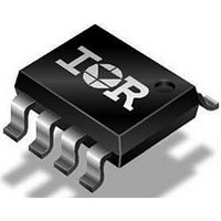
IRF7301 International Rectifier, IRF7301 Datasheet

IRF7301
Specifications of IRF7301
Available stocks
Related parts for IRF7301
IRF7301 Summary of contents
Page 1
... Junction and Storage Temperature Range J, STG Thermal Resistance Ratings Parameter R Maximum Junction-to-Ambient iew Max. @ 4.5V 5 4.5V 5 4.5V 4 2.0 0.016 ± 12 5.0 - 150 Typ. ––– 9.1238C IRF7301 V = 20V DSS R = 0.050 DS(on Units A W W/°C V V/ns °C Max. Units 62.5 °C/W 8/25/97 ...
Page 2
... IRF7301 Electrical Characteristics @ T Parameter V Drain-to-Source Breakdown Voltage (BR)DSS Breakdown Voltage Temp. Coefficient (BR)DSS J R Static Drain-to-Source On-Resistance DS(ON) V Gate Threshold Voltage GS(th) g Forward Transconductance fs I Drain-to-Source Leakage Current DSS Gate-to-Source Forward Leakage I GSS Gate-to-Source Reverse Leakage Q Total Gate Charge g Q Gate-to-Source Charge ...
Page 3
... Fig 1. Typical Output Characteristics ° ° µ te-to-S o urce V oltage ( Fig 3. Typical Transfer Characteristics TOP BOTT OM 1. Fig 2. Typical Output Characteristics . Fig 4. Normalized On-Resistance IRF7301 VGS 7.5V 5.0V 4.0V 3.5V 3.0V 2.5V 2.0V 1 µ LSE 0° Drain-to-Source V oltage ( 4 Junction Temperature (° Vs. Temperature ...
Page 4
... IRF7301 0V iss rss oss rss Drain-to-Source V oltage ( Fig 5. Typical Capacitance Vs. Drain-to-Source Voltage 50° 5° Source-to-D rain Voltage ( Fig 7. Typical Source-Drain Diode Forward Voltage . TED Fig 6. Typical Gate Charge Vs. 100 150 C J Single Pulse 0 Fig 8. Maximum Safe Operating Area = TEST C IRC U IT ...
Page 5
... Fig 11. Maximum Effective Transient Thermal Impedance, Junction-to-Ambient 4.5V Pulse Width Duty Factor Fig 10a. Switching Time Test Circuit V DS 90% 10% 125 150 V GS ° d(on) Fig 10b. Switching Time Waveforms Notes: 1. Duty factor Peak 0.01 0 Rectangular Pulse Duration (sec) 1 IRF7301 D.U. µ d(off ...
Page 6
... IRF7301 Charge Fig 12a. Basic Gate Charge Waveform Current Regulator Same Type as D.U.T. 50K .2 F 12V .3 F D.U. 3mA Current Sampling Resistors Fig 12b. Gate Charge Test Circuit + ...
Page 7
... Logic Level and 3V Drive Devices GS Fig 13. For N-Channel HEXFETS Circuit Layout Considerations Low Stray Inductance Ground Plane Low Leakage Inductance Current Transformer - + dv/dt controlled controlled by Duty Factor "D" SD D.U.T. - Device Under Test P. Period [ V =10V GS Current di/dt Diode Recovery dv/ Forward Drop [ ] IRF7301 + * *** ...
Page 8
... IRF7301 Package Outline SO8 Outline 0.25 (.010 0.25 (.010 Part Marking Information SO8 101 101 ° INCHES MILLIMETERS DIM MIN MAX MIN MAX A .0532 .0688 1.35 1.75 A1 .0040 .0098 0.10 0.25 B .014 .018 0.36 0.46 C .0075 .0098 0.19 0.25 D .189 .196 4 ...
Page 9
... IR FAR EAST: K&H Bldg., 2F, 30-4 Nishi-Ikebukuro 3-Chome, Toshima-Ku, Tokyo Japan 171 Tel 3983 0086 IR SOUTHEAST ASIA: 315 Outram Road, #10-02 Tan Boon Liat Building, Singapore 0316 Tel: 65 221 8371 http://www.irf.com .00 ( ITALY: Via Liguria 49, 10071 Borgaro, Torino Tel 451 0111 Data and specifications subject to change without notice. IRF7301 . . 4 2 8/97 ...


