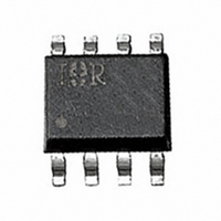
IRF7521D1 International Rectifier, IRF7521D1 Datasheet

IRF7521D1
Specifications of IRF7521D1
Available stocks
Related parts for IRF7521D1
IRF7521D1 Summary of contents
Page 1
... Surface mounted on FR-4 board, t www.irf.com PRELIMINARY FETKY MOSFET / Schottky Diode Power MOSFET will allow it to fit easily into extremely thin = 25°C unless otherwise noted 4. 150°C (BR)DSS J 2% 10sec. PD-91646C IRF7521D1 20V DSS 0.135 DS(on Schottky Vf = 0.39V TM Micro8 TM Maximum Units 2.4 A 1.9 19 1.3 W ...
Page 2
... IRF7521D1 MOSFET Electrical Characteristics @ T Parameter V Drain-to-Source Breakdown Voltage (BR)DSS R Static Drain-to-Source On-Resistance DS(on) V Gate Threshold Voltage GS(th) g Forward Transconductance fs I Drain-to-Source Leakage Current DSS Gate-to-Source Forward Leakage I GSS Gate-to-Source Reverse Leakage Q Total Gate Charge g Q Gate-to-Source Charge gs Q Gate-to-Drain ("Miller") Charge ...
Page 3
... Power Mosfet Characteristics 0.1 1 .5V 20 µ 5° 0. 2.0 1.5 1.0 0 µ 0.0 A 3.0 3.5 4.0 IRF7521D1 VGS TOP 7.5V 5.0V 4.0V 3.5V 3.0V 2.5V 2.0V BOTTOM 1. .5V 2 0µ 0° rain-to-S ource V oltage ( Fig 2. Typical Output Characteristics -60 -40 -20 ...
Page 4
... IRF7521D1 iss oss rss rain-to-S ourc e V oltage ( Fig 5. Typical Capacitance Vs. Drain-to-Source Voltage ° ° 0.1 0.4 0.6 0.8 1.0 1 ourc e-to-D rain V oltage ( Fig 7. Typical Source-Drain Diode Forward Voltage 4 Power Mosfet Characteristics . Fig 6. Typical Gate Charge Vs ing lse 0.1 1.4 1 ...
Page 5
... rain C urrent (A) D Fig 10. Typical On-Resistance Vs. Drain Current www.irf.com Power Mosfet Characteristics 0.001 0.01 0 Rectangular Pulse Duration (sec 5. 4. 0.0 5.0 6.0 7.0 Fig 11. Typical On-Resistance Vs. Gate IRF7521D1 Notes: 1. Duty factor Peak thJC 1.7A D 2.0 4.0 6 Gate-to-Source Voltage ( Voltage ...
Page 6
... IRF7521D1 Schottky Diode Characteristics 0.1 0.0 0.2 0.4 0.6 Forwa lta Forward Votage Drop - V Fig. 12 -Typical Forward Voltage Drop Characteristics ° ° ° 0.8 1 era ge Forw ard C urrent - I Fig.14 - Maximum Allowable Ambient J R Fig Typical Values of Reverse Current Vs. Reverse Voltage V = 20V ...
Page 7
... 0.0 8 (.0 03 DIME N S ION . DIME N S ION : INC DIME N S ION INC Part Marking www.irf.com SSIGN UAL 0.10 (.004 IRF7521D1 INC ILLIME MIN .044 0 .91 1. .008 0 .10 0. .014 0 .25 0.36 C .005 .007 0.13 0.18 D .116 .120 2.95 3.05 e .0256 B ASIC ...
Page 8
... IRF7521D1 TM Micro8 Tape & Reel & & WORLD HEADQUARTERS: 233 Kansas St., El Segundo, California 90245, Tel: (310) 322 3331 IR GREAT BRITAIN: Hurst Green, Oxted, Surrey RH8 9BB, UK Tel 1883 732020 IR GERMANY: Saalburgstrasse 157, 61350 Bad Homburg Tel 6172 96590 IR FAR EAST: K&H Bldg., 2F, 30-4 Nishi-Ikebukuro 3-Chome, Toshima-Ku, Tokyo Japan 171 Tel 3983 0086 IR SOUTHEAST ASIA: 1 Kim Seng Promenade, Great World City West Tower, 13-11, Singapore 237994 Tel 221 8371 IR TAIWAN:16 Fl ...


