IRF9953 International Rectifier, IRF9953 Datasheet
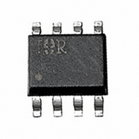
MOSFET 2P-CH 30V 2.3A 8-SOIC

IRF9953

Manufacturer Part Number
IRF9953
Description
MOSFET 2P-CH 30V 2.3A 8-SOIC
Manufacturer
International Rectifier
Series
HEXFET®r
Datasheet

Specifications of IRF9953

Fet Type
2 P-Channel (Dual)
Fet Feature
Logic Level Gate
Rds On (max) @ Id, Vgs
250 mOhm @ 1A, 10V
Drain To Source Voltage (vdss)
30V
Current - Continuous Drain (id) @ 25° C
2.3A
Vgs(th) (max) @ Id
1V @ 250µA
Gate Charge (qg) @ Vgs
12nC @ 10V
Input Capacitance (ciss) @ Vds
190pF @ 15V
Power - Max
2W
Mounting Type
Surface Mount
Package / Case
8-SOIC (3.9mm Width)
Lead Free Status / RoHS Status
Contains lead / RoHS non-compliant
Other names
*IRF9953

Available stocks

Company
Part Number
Manufacturer
Quantity
Price
Part Number:
IRF9953
Quantity:
5 000
Part Number:
IRF9953PBF
Manufacturer:
IR
Quantity:
20 000
Part Number:
IRF9953TRPBF
Manufacturer:
International Rectifier
Quantity:
31 817
Part Number:
IRF9953TRPBF
Manufacturer:
IR
Quantity:
8 000
Part Number:
IRF9953TRPBF
Manufacturer:
IR
Quantity:
20 000
Company:
Part Number:
IRF9953TRPBF
Quantity:
9 000
Fifth Generation HEXFETs from International Rectifier
utilize advanced processing techniques to achieve
extremely low on-resistance per silicon area. This
benefit, combined with the fast switching speed and
ruggedized device design that HEXFET Power
MOSFETs are well known for, provides the designer
with an extremely efficient and reliable device for use
in a wide variety of applications.
The SO-8 has been modified through a customized
leadframe for enhanced thermal characteristics and
multiple-die capability making it ideal in a variety of
power applications. With these improvements, multiple
devices can be used in an application with dramatically
reduced board space. The package is designed for
vapor phase, infra red, or wave soldering techniques.
Absolute Maximum Ratings ( T
Thermal Resistance Ratings
Description
Maximum Power Dissipation
Drain-Source Voltage
Gate-Source Voltage
Continuous Drain Current
Pulsed Drain Current
Continuous Source Current (Diode Conduction)
Single Pulse Avalanche Energy
Avalanche Current
Repetitive Avalanche Energy
Peak Diode Recovery dv/dt
Junction and Storage Temperature Range
Maximum Junction-to-Ambient
Generation V Technology
Ultra Low On-Resistance
Dual P-Channel MOSFET
Surface Mount
Very Low Gate Charge and
Switching Losses
Fully Avalanche Rated
Parameter
A
= 25°C Unless Otherwise Noted)
T
T
T
T
A
A
A
A
PRELIMINARY
= 25°C
= 70°C
= 25°C
= 70°C
Recommended upgrade: IRF7306 or IRF7316
Lower profile/smaller equivalent: IRF7506
G 2
G 1
S 2
S 1
Symbol
T
J,
dv/dt
V
V
E
E
I
I
DM
I
AR
T
GS
DS
AS
AR
S
1
2
3
4
STG
T op V iew
Symbol
R
HEXFET
JA
8
7
6
5
-55 to + 150
Maximum
D 1
D 1
D 2
D 2
± 20
0.20
S O -8
-1.3
-5.0
-30
-2.3
-1.8
-10
1.6
2.0
1.3
57
®
IRF9953
R
Limit
Power MOSFET
62.5
V
DS(on)
DSS
PD - 9.1560A
= -30V
= 0.25
Units
Units
°C/W
V/ ns
mJ
mJ
°C
W
A
A
8/25/97

Related parts for IRF9953

IRF9953 Summary of contents

Page 1

... Recommended upgrade: IRF7306 or IRF7316 Lower profile/smaller equivalent: IRF7506 = 25°C Unless Otherwise Noted) A Symbol 25° 70° 25° 70° dv/ STG Symbol 9.1560A IRF9953 ® HEXFET Power MOSFET -30V DSS 0. DS(on Maximum Units -30 ± 20 -2.3 -1.8 A -10 1.6 2 -1.3 A 0. 150 ° ...

Page 2

... IRF9953 Electrical Characteristics @ T Parameter V Drain-to-Source Breakdown Voltage (BR)DSS Breakdown Voltage Temp. Coefficient (BR)DSS J R Static Drain-to-Source On-Resistance DS(on) V Gate Threshold Voltage GS(th) g Forward Transconductance fs I Drain-to-Source Leakage Current DSS Gate-to-Source Forward Leakage I GSS Gate-to-Source Reverse Leakage Q Total Gate Charge g Q Gate-to-Source Charge ...

Page 3

... D rain-to-S ource V oltage ( Fig 1. Typical Output Characteristics ° ° µ te-to-S o urce V oltage ( Fig 3. Typical Transfer Characteristics -3 IRF9953 VGS TOP - 15V - 10V - 7.0V - 5.5V - 4.5V - 4.0V - 3.5V BOTT µ LSE W IDTH 0° rain-to-S ource V oltage ( Fig 2. Typical Output Characteristics ° ° ...

Page 4

... IRF9953 2.0 -1. 1.5 1.0 0.5 0.0 -60 -40 - 100 120 140 160 T , Junction Temperature ( C) J Fig 5. Normalized On-Resistance Vs. Temperature ate -to-S ource V oltage ( Fig 7. Typical On-Resistance Vs. Gate Voltage -10V ° Fig 6. Typical On-Resistance Vs. Drain 150 120 I = -2. rain C urrent ( Current 100 Starting T , Junction Temperature ( C) J Fig 8 ...

Page 5

... SINGLE PULSE (THERMAL RESPONSE) 0.1 0.00001 0.0001 Fig 11. Maximum Effective Transient Thermal Impedance, Junction-to-Ambient TED 0.001 0. Rectangular Pulse Duration (sec) 1 IRF9953 I = -2. Total Gate Charge (nC) G Fig 10. Typical Gate Charge Vs. Gate-to-Source Voltage P DM Notes: 1. Duty factor Peak ...

Page 6

... IRF9953 Package Outline SO8 Outline 0.25 (. 0.25 ( .010 IME NS IO NING AND NCING 14.5M- 1982 LLING D IME CH IME ILLIME (INC TLIN TLINE MS -01 2AA . 5 DIM ENS INCLU RUS TRU SIO XCEE D 0.25 (.006). DIM ENS LDE RIN E.. 6 Part Marking Information ...

Page 7

... IR SOUTHEAST ASIA: 315 Outram Road, #10-02 Tan Boon Liat Building, Singapore 0316 Tel: 65 221 8371 http://www.irf.com .00 ( GERMANY: Saalburgstrasse 157, 61350 Bad Homburg Tel 6172 96590 IR ITALY: Via Liguria 49, 10071 Borgaro, Torino Tel 451 0111 Data and specifications subject to change without notice. IRF9953 . . 4 2 8/97 ...

Related keywords