IRFB3307 International Rectifier, IRFB3307 Datasheet
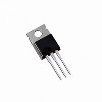
MOSFET N-CH 75V 130A TO-220AB

IRFB3307

Manufacturer Part Number
IRFB3307
Description
MOSFET N-CH 75V 130A TO-220AB
Manufacturer
International Rectifier
Series
HEXFET®r
Datasheet

Specifications of IRFB3307

Fet Type
MOSFET N-Channel, Metal Oxide
Fet Feature
Standard
Rds On (max) @ Id, Vgs
6.3 mOhm @ 75A, 10V
Drain To Source Voltage (vdss)
75V
Current - Continuous Drain (id) @ 25° C
130A
Vgs(th) (max) @ Id
4V @ 150µA
Gate Charge (qg) @ Vgs
180nC @ 10V
Input Capacitance (ciss) @ Vds
5150pF @ 50V
Power - Max
250W
Mounting Type
Through Hole
Package / Case
TO-220-3 (Straight Leads)
Lead Free Status / RoHS Status
Contains lead / RoHS non-compliant
Other names
*IRFB3307

Available stocks

Company
Part Number
Manufacturer
Quantity
Price
Part Number:
IRFB3307
Manufacturer:
IR
Quantity:
12 500
Part Number:
IRFB3307PBF
Manufacturer:
IR
Quantity:
20 000
Company:
Part Number:
IRFB3307PBF
Quantity:
20
Company:
Part Number:
IRFB3307PBF
Quantity:
1 000
Part Number:
IRFB3307ZPBF
Manufacturer:
IR
Quantity:
12 500
Part Number:
IRFB3307ZPBF
Manufacturer:
IR
Quantity:
20 000
Part Number:
IRFB3307ZPBF
0
Company:
Part Number:
IRFB3307ZPBF
Quantity:
9 000
Company:
Part Number:
IRFB3307ZPBF
Quantity:
25 780
Applications
l
l
l
l
Benefits
l
l
l
www.irf.com
Absolute Maximum Ratings
I
I
I
P
V
dv/dt
T
T
Avalanche Characteristics
E
I
E
Thermal Resistance
R
R
R
R
D
D
DM
AR
D
GS
J
STG
AS (Thermally limited)
AR
θJC
θCS
θJA
θJA
High Efficiency Synchronous Rectification in SMPS
Uninterruptible Power Supply
High Speed Power Switching
Hard Switched and High Frequency Circuits
@ T
@ T
Improved Gate, Avalanche and Dynamic dV/dt
Ruggedness
Fully Characterized Capacitance and Avalanche
Enhanced body diode dV/dt and dI/dt Capability
SOA
@T
Symbol
Symbol
C
C
C
= 25°C
= 100°C
= 25°C
Continuous Drain Current, V
Pulsed Drain Current
Maximum Power Dissipation
Linear Derating Factor
Gate-to-Source Voltage
Peak Diode Recovery
Operating Junction and
Storage Temperature Range
Soldering Temperature, for 10 seconds
(1.6mm from case)
Mounting torque, 6-32 or M3 screw
Single Pulse Avalanche Energy
Avalanche Current
Repetitive Avalanche Energy
Junction-to-Case
Case-to-Sink, Flat Greased Surface , TO-220
Junction-to-Ambient, TO-220
Junction-to-Ambient (PCB Mount) , D
Parameter
Parameter
k
Ù
f
GS
GS
k
g
@ 10V
@ 10V
e
2
Pak
jk
G
TO-220AB
IRFB3307
G
D
S
D
S
Typ.
See Fig. 14, 15, 16a, 16b
0.50
–––
–––
–––
V
R
I
D
DSS
DS(on)
10lb
-55 to + 175
x
IRFS3307
in (1.1N
130
Max.
91
HEXFET Power MOSFET
510
250
± 20
300
270
1.6
D
11
2
Pak
G
typ.
max.
D
x
m)
S
Max.
0.61
–––
62
40
IRFSL3307
IRFB3307
IRFS3307
5.0m
6.3m
130A
75V
IRFSL3307
TO-262
Units
Units
W/°C
°C/W
V/ns
G
mJ
mJ
°C
W
A
V
A
01/20/06
D
1
S

Related parts for IRFB3307

IRFB3307 Summary of contents

Page 1

... R Case-to-Sink, Flat Greased Surface , TO-220 θCS R Junction-to-Ambient, TO-220 θJA R Junction-to-Ambient (PCB Mount θJA www.irf.com G TO-220AB IRFB3307 Parameter @ 10V GS @ 10V Ù g Parameter Pak IRFB3307 IRFS3307 IRFSL3307 HEXFET Power MOSFET D V 75V DSS R typ. 5.0m DS(on) max. 6.3m I 130A Pak IRFS3307 IRFSL3307 Max. ™ ...

Page 2

Static @ T = 25°C (unless otherwise specified) J Symbol Parameter V Drain-to-Source Breakdown Voltage (BR)DSS ∆V /∆T Breakdown Voltage Temp. Coefficient (BR)DSS J R Static Drain-to-Source On-Resistance DS(on) V Gate Threshold Voltage GS(th) I Drain-to-Source Leakage Current DSS I ...

Page 3

PULSE WIDTH Tj = 25°C 0.01 0 Drain-to-Source Voltage (V) Fig 1. Typical Output Characteristics 1000 100 175° 25°C 1 ...

Page 4

175°C 100 25° 0.2 0.4 0.6 0.8 1.0 1.2 1.4 1.6 1.8 2 Source-to-Drain Voltage (V) Fig 7. Typical Source-Drain Diode Forward Voltage 140 120 Limited By Package ...

Page 5

D = 0.50 0.20 0.1 0.10 0.05 0.02 0.01 0.01 SINGLE PULSE ( THERMAL RESPONSE ) 0.001 0.0001 1E-006 1E-005 Fig 13. Maximum Effective Transient Thermal Impedance, Junction-to-Case 100 Duty Cycle = Single Pulse 10 1 Allowed avalanche Current ...

Page 6

150µA 3 250µ 1.0mA 2 1.0A 2.0 1.5 -75 -50 - 100 125 150 175 200 Temperature ...

Page 7

D.U.T + ƒ ‚ -  • • • SD • Fig 20 D.U 20V V GS 0.01 Ω Fig 21a. Unclamped Inductive Test Circuit ...

Page 8

EXAMPLE: T HIS IS AN IRF1010 LOT CODE 1789 AS S EMBLED ON WW 19, 2000 EMBLY LINE "C" Note: "P" in ass embly line position indicates "Lead - Free" TO-220AB packages are not recommended ...

Page 9

TO-262 Package Outline Dimensions are shown in millimeters (inches) TO-262 Part Marking Information EXAMPLE: T HIS IS AN IRL3103L LOT CODE 1789 AS S EMBLED ON WW 19, 1997 EMBLY LINE "C" www.irf.com INT ERNATIONAL ...

Page 10

T HIS IS AN IRF530S WITH LOT CODE 8024 ASS EMBLED ON WW 02, 2000 ASS EMBLY LINE "L" INT ERNAT IONAL RECT IFIER LOGO ASS EMBLY LOT CODE INT ERNAT IONAL RECT ...

Page 11

TRR FEED DIRECTION 1.85 (.073) 1.65 (.065) TRL FEED DIRECTION 330.00 (14.173) MAX. NOTES : 1. COMFORMS TO EIA-418. 2. CONTROLLING DIMENSION: MILLIMETER. 3. DIMENSION MEASURED @ HUB. 4. INCLUDES FLANGE DISTORTION @ OUTER EDGE. IR WORLD HEADQUARTERS: 233 ...

Page 12

Note: For the most current drawings please refer to the IR website at: http://www.irf.com/package/ ...

Related keywords