LF411CN/NOPB National Semiconductor, LF411CN/NOPB Datasheet
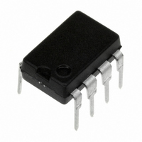
IC OP AMP LOW JFET INPUT 8-DIP

LF411CN/NOPB

Manufacturer Part Number
LF411CN/NOPB
Description
IC OP AMP LOW JFET INPUT 8-DIP
Manufacturer
National Semiconductor
Series
BI-FET II™r
Datasheets

Specifications of LF411CN/NOPB

Amplifier Type
J-FET
Number Of Circuits
1
Slew Rate
15 V/µs
Gain Bandwidth Product
4MHz
Current - Input Bias
50pA
Voltage - Input Offset
800µV
Current - Supply
1.8mA
Voltage - Supply, Single/dual (±)
10 V ~ 36 V, ±5 V ~ 18 V
Operating Temperature
0°C ~ 70°C
Mounting Type
Through Hole
Package / Case
8-DIP (0.300", 7.62mm)
Bandwidth
4 MHz
Common Mode Rejection Ratio
100
Current, Input Bias
50 pA
Current, Input Offset
25 pA
Current, Output
25 mA
Current, Supply
1.8 mA
Harmonic Distortion
0.02 %
Impedance, Thermal
120 °C/W
Number Of Amplifiers
Single
Package Type
MDIP-8
Power Dissipation
670 mW
Resistance, Input
10^12 Ohms
Temperature, Operating, Range
0 to +70 °C
Voltage, Gain
200 V/mV
Voltage, Input
10 to 44 V
Voltage, Noise
25 nV/sqrt Hz
Voltage, Offset
0.8 mV
Voltage, Output, High
13.5 V
Voltage, Output, Low
-13.5 V
Voltage, Supply
±15 V
Number Of Channels
1
Voltage Gain Db
106.02 dB
Common Mode Rejection Ratio (min)
70 dB
Input Voltage Range (max)
44 V
Input Voltage Range (min)
10 V
Input Offset Voltage
2 mV at +/- 15 V
Supply Current
3.4 mA at +/- 15 V
Maximum Power Dissipation
670 mW
Maximum Operating Temperature
+ 70 C
Mounting Style
Through Hole
Maximum Dual Supply Voltage
+/- 18 V
Minimum Operating Temperature
0 C
Lead Free Status / RoHS Status
Lead free / RoHS Compliant
Output Type
-
Current - Output / Channel
-
-3db Bandwidth
-
Lead Free Status / Rohs Status
RoHS Compliant part Electrostatic Device
Other names
*LF411CN
*LF411CN/NOPB
LF411
LF411CN

Available stocks

Company
Part Number
Manufacturer
Quantity
Price
Part Number:
LF411CN/NOPB
Manufacturer:
NS
Quantity:
9 980
© 2004 National Semiconductor Corporation
LF411
Low Offset, Low Drift JFET Input Operational Amplifier
General Description
These devices are low cost, high speed, JFET input opera-
tional amplifiers with very low input offset voltage and guar-
anteed input offset voltage drift. They require low supply
current yet maintain a large gain bandwidth product and fast
slew rate. In addition, well matched high voltage JFET input
devices provide very low input bias and offset currents. The
LF411 is pin compatible with the standard LM741 allowing
designers to immediately upgrade the overall performance of
existing designs.
These amplifiers may be used in applications such as high
speed integrators, fast D/A converters, sample and hold
circuits and many other circuits requiring low input offset
voltage and drift, low input bias current, high input imped-
ance, high slew rate and wide bandwidth.
Typical Connection
Ordering Information
X indicates electrical grade
Y indicates temperature range
Z indicates package type
BI-FET II
LF411XYZ
“M” for military
“C” for commercial
“H” or “N”
is a trademark of National Semiconductor Corporation.
DS005655
00565501
Features
n Internally trimmed offset voltage:
n Input offset voltage drift:
n Low input bias current:
n Low input noise current:
n Wide gain bandwidth:
n High slew rate:
n Low supply current:
n High input impedance:
n Low total harmonic distortion:
n Low 1/f noise corner:
n Fast settling time to 0.01%:
Connection Diagrams
Note: Pin 4 connected to case.
Order Number LF411ACN, LF411CN
See NS Package Number H08A
See NS Package Number N08E
Order Number LF411ACH
or LF411MH/883 (Note 11)
Dual-In-Line Package
Metal Can Package
Top View
Top View
00565507
00565505
10 µV/˚C(max)
www.national.com
0.5 mV(max)
August 2000
0.01 pA/
10V/µs(min)
3 MHz(min)
≤0.02%
1.8 mA
10
50 pA
50 Hz
2 µs
12
Hz

Related parts for LF411CN/NOPB

LF411CN/NOPB Summary of contents

Page 1

... Z indicates package type “H” or “N” BI-FET II ™ trademark of National Semiconductor Corporation. © 2004 National Semiconductor Corporation Features n Internally trimmed offset voltage: n Input offset voltage drift: n Low input bias current: n Low input noise current: ...

Page 2

... Absolute Maximum Ratings If Military/Aerospace specified devices are required, please contact the National Semiconductor Sales Office/ Distributors for availability and specifications. LF411A Supply Voltage Differential Input Voltage Input Voltage Range (Note 2) Output Short Circuit Duration Continuous Continuous H Package Power Dissipation (Notes 3, 10) ...

Page 3

AC Electrical Characteristic Symbol Parameter THD Total Harmonic Distortion Note 1: “Absolute Maximum Ratings” indicate limits beyond which damage to the device may occur. Operating Ratings indicate conditions for which the device is functional, but do not guarantee specific performance ...

Page 4

Typical Performance Characteristics Supply Current Negative Common-Mode Input Voltage Limit Negative Current Limit www.national.com (Continued) Positive Common-Mode Input Voltage Limit 00565513 Positive Current Limit 00565515 Output Voltage Swing 00565517 4 00565514 00565516 00565518 ...

Page 5

Typical Performance Characteristics Output Voltage Swing Bode Plot Distortion vs Frequency (Continued) 00565519 00565521 00565523 5 Gain Bandwidth 00565520 Slew Rate 00565522 Undistorted Output Voltage Swing 00565524 www.national.com ...

Page 6

Typical Performance Characteristics Open Loop Frequency Response Power Supply Rejection Ratio Open Loop Voltage Gain www.national.com (Continued) Common-Mode Rejection 00565525 Equivalent Input Noise 00565527 Output Impedance 00565529 6 Ratio 00565526 Voltage 00565528 00565530 ...

Page 7

Typical Performance Characteristics Inverter Settling Time Pulse Response R =2 kΩ Small Signal Inverting Small Signal Non-Inverting (Continued) 00565531 00565539 00565540 7 Large Signal Inverting 00565541 Large Signal Non-Inverting 00565542 www.national.com ...

Page 8

Pulse Response R =2 kΩ Application Hints The LF411 series of internally trimmed JFET input op amps ( BI-FET II ™ ) provide very low input offset voltage and guaranteed input offset voltage drift. These JFETs have large ...

Page 9

Typical Applications PNP=2N2905 NPN=2N2219 unless noted TO-5 heat sinks for Q6-Q7 High Speed Current Booster 9 00565509 www.national.com ...

Page 10

Typical Applications where the A digital input is high the A digital input is low N N www.national.com (Continued) 10-Bit Linear DAC with Single Supply Analog Switch with Buffered ...

Page 11

Simplified Schematic Note 11: Available per JM38510/11904 Detailed Schematic 00565506 11 00565534 www.national.com ...

Page 12

Physical Dimensions www.national.com inches (millimeters) unless otherwise noted Metal Can Package (H) Order Number LF411MH/883 or LF411ACH NS Package Number H08A Molded Dual-In-Line Package (N) Order Number LF411ACN or LF411CN NS Package Number N08E 12 ...

Page 13

... BANNED SUBSTANCE COMPLIANCE National Semiconductor certifies that the products and packing materials meet the provisions of the Customer Products Stewardship Specification (CSP-9-111C2) and the Banned Substances and Materials of Interest Specification (CSP-9-111S2) and contain no ‘‘Banned Substances’’ as defined in CSP-9-111S2. ...

Related keywords