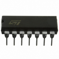
LM224AN STMicroelectronics, LM224AN Datasheet

LM224AN
Specifications of LM224AN
Available stocks
Related parts for LM224AN
LM224AN Summary of contents
Page 1
... Operation from split power supplies is also possible and the low power supply current drain is independent of the magnitude of the power supply voltage. Order codes Part number Temperature range LM224AN LM224AD/ADT -40° C, +105° C LM224APT LM324AN LM324AD/ADT 0° C, +70° C LM324APT ...
Page 2
Contents Contents 1 Pin connections and schematic diagram . . . . . . . . . . . . . . . . . . . . . . . . 3 2 Absolute maximum ratings . . . ...
Page 3
LM224A-LM324A 1 Pin connections and schematic diagram Figure 1. Pin connections (top view) Figure 2. Schematic diagram (1/4 LM124) Pin connections and schematic diagram 3/20 ...
Page 4
Absolute maximum ratings 2 Absolute maximum ratings Table 1. Absolute maximum ratings Symbol V Supply voltage CC V Input voltage i V Differential input voltage id Power dissipation suffix tot D suffix Output short-circuit duration I Input current ...
Page 5
LM224A-LM324A 3 Electrical characteristics Table specified) Symbol Input offset voltage +25° amb ≤ min Input offset current +25° amb ≤ min Input bias ...
Page 6
Electrical characteristics Table specified) Symbol High level output voltage +25°C amb ≤ min +25° amb ≤ min V = ...
Page 7
LM224A-LM324A Figure 3. Input bias current vs. ambient temperature INPUT BIAS CURRENT versus AMBIENT TEMPERATURE 24 IB (nA -55-35- 105 125 AMBIENT TEMPERATURE (°C) Figure 5. Input ...
Page 8
Electrical characteristics Figure 9. Input bias current vs. ambient temperature INPUT BIAS CURRENT versus AMBIENT TEMPERATURE 24 IB (nA -55-35- 105 125 AMBIENT TEMPERATURE (°C) Figure 11. ...
Page 9
LM224A-LM324A Figure 15. Electrical curves Electrical characteristics 9/20 ...
Page 10
Electrical characteristics Figure 16. Input current Figure 18. Power supply & common mode rejection ratio 10/20 Figure 17. Large signal voltage gain Figure 19. Voltage gain LM224A-LM324A ...
Page 11
LM224A-LM324A 4 Typical single-supply applications Figure 20. AC coupled inverting amplifier Figure 22. AC coupled non inverting amplifier Figure 24. Non-inverting DC gain Typical single-supply applications Figure 21. High input Z adjustable gain DC instrumentation amplifier ...
Page 12
Typical single-supply applications Figure 26. Active bandpass filter Fo = 1kHz 100 (40dB) Figure 28. Using symmetrical amplifiers to reduce input current (general concept) 12/20 Figure 27. High input Z, DC differential amplifier R R ...
Page 13
LM224A-LM324A 5 Macromodels Note: Please consider the following before using this macromodel: All models are a trade-off between accuracy and complexity (i.e. simulation time). Macromodels are not a substitute to breadboarding; rather, they confirm the validity of a design approach ...
Page 14
Macromodels FIP 5 19 VOFP 3.600000E+02 FIN 5 19 VOFN 3.600000E+02 RG1 19 5 3.652997E+06 RG2 19 4 3.652997E+ 6.000000E-09 DOPM 19 22 MDTH 400E-12 DONM 21 19 MDTH 400E-12 HOPM 22 28 VOUT 7.500000E+03 VIPM 28 ...
Page 15
... JEDEC Standard JESD97. The maximum ratings related to soldering conditions are also marked on the inner box label. ECOPACK is an STMicroelectronics trademark. ECOPACK specifications are available at: www.st.com. Package mechanical data ...
Page 16
Package mechanical data 6.1 DIP14 package DIM. MIN. a1 0. 1.27 16/20 Plastic DIP-14 MECHANICAL DATA mm. TYP MAX. MIN. 0.020 1.65 0.055 0.5 0.25 20 8.5 2.54 ...
Page 17
LM224A-LM324A 6.2 SO-14 package DIM. MIN 0. SO-14 MECHANICAL DATA mm. TYP MAX. 1.75 0.1 0.2 1.65 0.46 0.25 0.5 45˚ (typ.) ...
Page 18
Package mechanical data 6.3 TSSOP14 package DIM. MIN 0. 0. PIN 1 IDENTIFICATION 18/20 TSSOP14 MECHANICAL DATA mm. TYP MAX. 1.2 0.15 0.8 1 ...
Page 19
LM224A-LM324A 7 Revision history Table 4. Document revision history Date 1-Mar-2001 1-Feb-2005 1-Jun-2005 25-Sep-2006 Revision 1 First Release Added explanation Updated macromodel. 3 ESD protection inserted in 4 Editorial update. Revision history Changes and V limits in ...
Page 20
... Information in this document is provided solely in connection with ST products. STMicroelectronics NV and its subsidiaries (“ST”) reserve the right to make changes, corrections, modifications or improvements, to this document, and the products and services described herein at any time, without notice. All ST products are sold pursuant to ST’s terms and conditions of sale. ...


