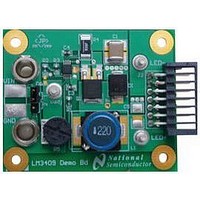
LM3409HVEVAL/NOPB National Semiconductor, LM3409HVEVAL/NOPB Datasheet

LM3409HVEVAL/NOPB
Specifications of LM3409HVEVAL/NOPB
Related parts for LM3409HVEVAL/NOPB
LM3409HVEVAL/NOPB Summary of contents
Page 1
... This board can be easily modified to demonstrate other op- erating points as shown in the Alternate Designs section. The LM3409/09HV datasheet Design Procedure can be used to design for any set of specifications. Schematic © 2009 National Semiconductor Corporation National Semiconductor Application Note 1953 James Patterson November 20, 2009 EFFICIENCY WITH 12 SERIES LEDS AT 1 ...
Page 2
Pin Descriptions Pin(s) Name Description 1 UVLO Input under-voltage lockout 2 IADJ Analog LED current adjust 3 EN Logic level enable / PWM dimming 4 COFF Off-time programming 5 GND 6 PGATE 7 CSN Negative current sense 8 CSP Positive ...
Page 3
PCB Layout The 2 inner planes are GND and Top Layer Bottom Layer 3 30093540 30093541 www.national.com ...
Page 4
Design Procedure SPECIFICATIONS V = 48V 75V IN IN-MAX V = 42V 400kHz 1.5A LED Δi = Δi = 300mA LED-PP L-PP Δv = 1.44V IN- 10V 1.1V ...
Page 5
P-CHANNEL MOSFET Determine minimum Q1 voltage rating and current rating: A 100V 3.8A PFET is chosen with R DS-ON 20nC. Determine I and P : T-RMS T The chosen component from step 6 is: 7. RE-CIRCULATING DIODE Determine minimum ...
Page 6
PWM DIMMING METHOD The LM3409HV evaluation board allows for PWM dimming to be evaluated as follows: Method # PWM dimming is desired, a jumper should be placed in position 1 (shorts pins 1 and 2) on header ...
Page 7
Shunt FET Circuit Modification When the shunt FET (Q3) is on, the LM3409 is driving current into a short, therefore a maximum off-time (typical 300 µs) occurs followed by a minimum on-time. Maximum off-time followed by minimum on-time continues until ...
Page 8
Typical Waveforms T = +25° 48V and V = 42V 20kHz 50% EN pin PWM dimming 100kHz 50% External FET PWM dimming Analog dimming minimum (V www.national.com 30093543 20kHz 50% EN pin PWM dimming (rising ...
Page 9
Alternate Designs Alternate designs with the LM3409HV evaluation board are possible with very few changes to the existing hardware. The evaluation board FETs and diodes are already rated higher than necessary for design flexibility. The input UVLO can re- main ...
Page 10
... For more National Semiconductor product information and proven design tools, visit the following Web sites at: Products Amplifiers www.national.com/amplifiers Audio www.national.com/audio Clock and Timing www.national.com/timing Data Converters www.national.com/adc Interface www.national.com/interface LVDS www.national.com/lvds Power Management www.national.com/power Switching Regulators www.national.com/switchers LDOs www.national.com/ldo LED Lighting www ...


