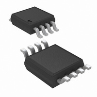
LMP2232AMM/NOPB National Semiconductor, LMP2232AMM/NOPB Datasheet

LMP2232AMM/NOPB
Specifications of LMP2232AMM/NOPB
Related parts for LMP2232AMM/NOPB
LMP2232AMM/NOPB Summary of contents
Page 1
... The LMP2231 is the single version of this product and the LMP2234 is the quad version of this product. Both of these products are available on National Semiconductor's website. Typical Application LMP ® registered trademark of National Semiconductor Corporation. © 2008 National Semiconductor Corporation Features (For V = 5V, Typical unless otherwise noted) S ■ ...
Page 2
... Absolute Maximum Ratings If Military/Aerospace specified devices are required, please contact the National Semiconductor Sales Office/ Distributors for availability and specifications. ESD Tolerance (Note 2) Human Body Model Machine Model Differential Input Voltage Supply Voltage ( – Voltage on Input/Output Pins Storage Temperature Range Junction Temperature (Note 3) ...
Page 3
Symbol Parameter G Gain Margin m e Input-Referred Voltage Noise Density n Input Referred Voltage Noise i Input-Referred Current Noise n THD+N Total Harmonic Distortion + Noise 3.3V DC Electrical Characteristics T = 25° 3.3V 0V, ...
Page 4
Symbol Parameter i Input-Referred Current Noise n THD+N Total Harmonic Distortion + Noise 2.5V DC Electrical Characteristics T = 25° 2.5V, V − Symbol Parameter V Input Offset Voltage OS TCV Input ...
Page 5
DC Electrical Characteristics T = 25° 1.8V 0V − Symbol Parameter V Input Offset Voltage OS TCV Input Offset Voltage Drift OS I Input Bias Current BIAS I Input ...
Page 6
Note 1: Absolute Maximum Ratings indicate limits beyond which damage may occur. Operating Ratings indicate conditions for which the device is intended to be functional, but specific performance is not guaranteed. For guaranteed specifications and test conditions, see the Electrical ...
Page 7
Typical Performance Characteristics − S Offset Voltage Distribution Offset Voltage Distribution Offset Voltage Distribution Unless otherwise Specified: T TCV 30033907 TCV 30033906 TCV 30033905 7 = 25° 5V /2, ...
Page 8
Offset Voltage Distribution Offset Voltage vs. V Offset Voltage vs. V www.national.com 30033973 CM 30033918 CM 30033964 8 TCV Distribution OS 30033969 Offset Voltage vs 30033965 Offset Voltage vs 30033972 ...
Page 9
Offset Voltage vs. Temperature 30033971 0 Voltage Noise 30033933 0 Voltage Noise 30033932 Offset Voltage vs. Supply Voltage 0 Voltage Noise 0 Voltage Noise ...
Page 10
Input Bias Current vs. V Input Bias Current vs. V Input Bias Current vs. V www.national.com Input Bias Current vs 30033955 Input Bias Current vs 30033957 Input Bias Current vs 30033959 10 CM 30033956 ...
Page 11
Input Bias Current vs 30033961 PSRR vs. Frequency 30033966 Sinking Current vs. Supply Voltage 30033913 Input Bias Current vs. V Supply Current vs. Supply Voltage (per channel) Sourcing Current vs. Supply Voltage 11 CM 30033962 30033912 30033914 www.national.com ...
Page 12
Output Swing High vs. Supply Voltage Open Loop Frequency Response Phase Margin vs. Capacitive Load www.national.com Output Swing Low vs. Supply Voltage 30033915 Open Loop Frequency Response 30033921 Slew Rate vs. Supply Voltage 30033963 12 30033916 30033922 30033930 ...
Page 13
THD+N vs. Amplitude 30033928 Large Signal Step Response 30033924 Large Signal Step Response 30033926 THD+N vs. Frequency Small Signal Step Response Small Signal Step Response 13 30033929 30033923 30033925 www.national.com ...
Page 14
CMRR vs. Frequency www.national.com Input Voltage Noise vs. Frequency 30033967 14 30033919 ...
Page 15
... Thus the LMP2232 provides better signal fidelity and a higher signal-to-noise ratio when interfacing with high impedance sensors. National Semiconductor is heavily committed to precision amplifiers and the market segments they serve. Technical support and extensive characterization data is available for sensitive applications or applications with a constrained error budget ...
Page 16
Figure 2 shows a schematic of this input voltage noise reduc- tion circuit. Typical resistor values are: R and kΩ. O FIGURE 2. Noise Reduction Circuit PRECISION INSTRUMENTATION AMPLIFIER Measurement of very small signals with an amplifier ...
Page 17
SINGLE SUPPLY STRAIN GAGE BRIDGE AMPLIFIER Strain gauges are popular electrical elements used to mea- sure force or pressure. Strain gauges are subjected to an unknown force which is measured as the deflection on a pre- viously calibrated scale. Pressure ...
Page 18
PORTABLE GAS DETECTION SENSOR Gas sensors are used in many different industrial and medical applications. They generate a current which is proportional to the percentage of a particular gas sensed in an air sample. This current goes through a load ...
Page 19
Physical Dimensions inches (millimeters) unless otherwise noted 8-Pin MSOP NS Package Number MUA08A 8-Pin SOIC NS Package Number M08A 19 www.national.com ...
Page 20
... For more National Semiconductor product information and proven design tools, visit the following Web sites at: Products Amplifiers www.national.com/amplifiers Audio www.national.com/audio Clock and Timing www.national.com/timing Data Converters www.national.com/adc Interface www.national.com/interface LVDS www.national.com/lvds Power Management www.national.com/power Switching Regulators www.national.com/switchers LDOs www.national.com/ldo LED Lighting www ...


