P0304 Terasic Technologies Inc, P0304 Datasheet
P0304
Specifications of P0304
Available stocks


Related parts for P0304


P0304 Summary of contents
Page 1
Altera DE2-70 Board Version 1.03 Copyright © 2008 Terasic Technologies ...
Page 2
Altera DE2-70 Board CONTENTS Chapter 1 DE2-70 Package ...............................................................................................................1 1.1 Package Contents .................................................................................................................1 1.2 The DE2-70 Board Assembly ..............................................................................................2 1.3 Getting Help.........................................................................................................................3 Chapter 2 Altera DE2-70 Board .......................................................................................................4 2.1 Layout and Components ......................................................................................................4 2.2 Block Diagram of the DE2-70 Board ...
Page 3
Altera DE2-70 Board 5.12 TV Decoder........................................................................................................................52 5.13 Implementing a TV Encoder..............................................................................................54 5.14 Using USB Host and Device..............................................................................................55 5.15 Using IrDA.........................................................................................................................56 5.16 Using SDRAM/SRAM/Flash.............................................................................................57 Chapter 6 Examples of Advanced Demonstrations ......................................................................66 6.1 DE2-70 Factory Configuration ..........................................................................................66 6.2 TV Box Demonstration......................................................................................................67 6.3 ...
Page 4
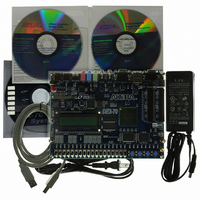
DE2-70 Package The DE2-70 package contains all components needed to use the DE2-70 board in conjunction with a computer that runs the Microsoft Windows software. 1.1 Package Contents Figure 1.1 shows a photograph of the DE2-70 package. Figure 1.1. The ...
Page 5
The DE2-70 package includes: The DE2-70 board USB Cable for FPGA programming and control DE2-70 System CD containing the DE2-70 documentation and supporting materials, including the User Manual, the Control Panel utility, reference designs and demonstrations, device ...
Page 6
Getting Help Here are the addresses where you can get help if you encounter problems: Altera Corporation 101 Innovation Drive San Jose, California, 95134 USA Email: university@altera.com Terasic Technologies No. 356, Sec. 1, Fusing E. Rd. Jhubei ...
Page 7
Altera DE2-70 Board This chapter presents the features and design characteristics of the DE2-70 board. 2.1 Layout and Components A photograph of the DE2-70 board is shown in Figure 2.1. It depicts the layout of the board and indicates the ...
Page 8
SSRAM Two 32-Mbyte SDRAM 8-Mbyte Flash memory SD Card socket 4 pushbutton switches 18 toggle switches 18 red user LEDs 9 green user LEDs 50-MHz ...
Page 9
Figure 2.2. Block diagram of the DE2-70 board. Following is more detailed information about the blocks in Figure 2.2: Cyclone II 2C70 FPGA 68,416 LEs 250 M4K RAM blocks 1,152,000 total RAM bits 150 embedded multipliers ...
Page 10
SSRAM 2-Mbyte standard synchronous SRAM Organized as 512K x 36 bits Accessible as memory for the Nios II processor and by the DE2-70 Control Panel SDRAM Two 32-Mbyte Single Data Rate Synchronous Dynamic RAM memory chips ...
Page 11
Audio CODEC Wolfson WM8731 24-bit sigma-delta audio CODEC Line-level input, line-level output, and microphone input jacks Sampling frequency KHz Applications for MP3 players and recorders, PDAs, smart phones, voice recorders, etc. VGA output ...
Page 12
Serial ports One RS-232 port One PS/2 port DB-9 serial connector for the RS-232 port PS/2 connector for connecting a PS2 mouse or keyboard to the DE2-70 board IrDA transceiver Contains a 115.2-kb/s infrared transceiver ...
Page 13
At this point you should observe the following: All user LEDs are flashing All 7-segment displays are cycling through the numbers The LCD display shows Welcome to the Altera DE2-70 The VGA monitor ...
Page 14
DE2-70 Control Panel The DE2-70 board comes with a Control Panel facility that allows users to access various components on the board from a host computer. The host computer communicates with the board through an USB connection. The facility can ...
Page 15
Quartus II to download a configuration file into the FPGA until you close the USB port. 7. The Control Panel is now ready for use; experiment by setting the value of some LEDs display ...
Page 16
Figure 3.2. The DE2-70 Control Panel concept. The DE2-70 Control Panel can be used to light up LEDs, change the values displayed on 7-segment and LCD displays, monitor buttons/switches status, read/write the SDRAM, SSRAM and Flash Memory, monitor the status ...
Page 17
Choosing the 7-SEG tab leads to the window in Figure 3.4. In the tab sheet, directly use the Up-Down control and Dot Check box to specified desired patterns, the 7-SEG patterns on the board will be updated immediately. Figure 3.4. ...
Page 18
Choosing the LCD tab leads to the window in Figure 3.5. Text can be written to the LCD display by typing it in the LCD box and pressing the Set button. Figure 3.5. Controlling LEDs and the LCD display. The ...
Page 19
Figure 3.6. Monitoring switches and buttons. The ability to check the status of button and switch is not needed in typical design activities. However, it provides users a simple mechanism for verifying if the buttons and switches are functioning correctly. ...
Page 20
Figure 3.7. Accessing the SDRAM-U1. A 16-bit word can be written into the SDRAM by entering the address of the desired location, specifying the data to be written, and pressing the Write button. Contents of the location can be read ...
Page 21
The Sequential Read function is used to read the contents of the SDRAM-U1 and place them into a file as follows: 1. Specify the starting address in the Address box. 2. Specify the number of bytes to ...
Page 22
Figure 3.8. USB Mouse Monitoring Tool. 3.6 PS2 Device The Control Panel provides users a tool to receive the inputs from a PS2 keyboard in real time. The received scan-codes are translated to ASCII code and displayed in the control ...
Page 23
Figure 3.9. Reading the PS2 Keyboard. 3.7 SD CARD The function is designed to read the identification and specification of the SD card. The 1-bit SD MODE is used to access the SD card. This function can be used to ...
Page 24
Figure 3.10. Reading the SD card Identification and Specification. 3.8 Audio Playing and Recording This interesting audio tool is designed to control the audio chip on the DE2-70 board for audio playing and recording. It can play audio stored in ...
Page 25
Figure 3.11. Playing audio from a selected wave file To record sound using a microphone, please follow the steps below: 1. Plug a microphone to the MIC port on the board. 2. Select the “Record MIC” item in the com-box ...
Page 26
Figure 3.12. Audio Recording and Saving as a WAV file. To record audio sound from LINE-IN port, please connect an audio source to the LINE-IN port on the board. The operation is as same as recording audio from MIC. 3.9 ...
Page 27
FPGA/ SOPC NIOS II TIMER JTAG JTAG Blaster Hardware Figure 3.13. The block diagram of the DE2-70 control panel. SEG7 Controller SDRAM Controller SDRAM Controller LCD Controller USB Controller PS2 Controller PIO Controller Avalon- MM Flash Controller Tris tate Bridge ...
Page 28
DE2-70 Video Utility The DE2-70 board comes with a video utility that allows users to access video components on the board from a host computer. The host computer communicates with the board through the USB-Blaster link. The facility can be ...
Page 29
Figure 4.1. The DE2-70 Video Utility window. 4.2 VGA Display Choosing the Display tab in the DE2-70 Video Utility leads to the window shown in Figure 4.2. The function is designed to download an image from the host computer to ...
Page 30
Figure 4.2. Displaying selected image file on VGA Monitor. 4.3 Video Capture Choosing the Capture tab leads to the window in Figure 4.3. The function is designed to capture an image from the video sources, and sent the image from ...
Page 31
Overall Structure of the DE2-70 Video Utility The DE2-70 Video Utility is based on a NIOS II system running in the Cyclone II FPGA with the SDRAM-U2 or SSRAM. The software part is implemented in C code; the hardware ...
Page 32
FPGA SOPC NIOS II TIMER JTAG JTAG Blaster Hardware Figure 4.4. Video Capture Block Diagram. The control flow for video displaying is described below: 1. Host computer downloads the raw image data to SDRAM-U2. 2. Host issues a “display” command ...
Page 33
Using the DE2-70 Board This chapter gives instructions for using the DE2-70 board and describes each of its I/O devices. 5.1 Configuring the Cyclone II FPGA The procedure for downloading a circuit from a host computer to the DE2-70 board ...
Page 34
Configuring the FPGA in JTAG Mode Figure 5.1 illustrates the JTAG configuration setup. To download a configuration bit stream into the Cyclone II FPGA, perform the following steps: Ensure that power is applied to the DE2-70 board Connect ...
Page 35
EPCS16 device to be loaded into the FPGA chip. USB Blaster Circuit USB Quartus II MAX ...
Page 36
There are also 18 toggle switches (sliders) on the DE2-70 board. These switches are not debounced, and are intended for use as level-sensitive data inputs to a circuit. Each switch is connected directly to a pin on the Cyclone II ...
Page 37
Figure 5.5. Schematic diagram of the LEDs. Signal Name FPGA Pin No. SW[0] PIN_AA23 SW[1] PIN_AB26 SW[2] PIN_AB25 SW[3] PIN_AC27 SW[4] PIN_AC26 SW[5] PIN_AC24 SW[6] PIN_AC23 SW[7] PIN_AD25 SW[8] PIN_AD24 SW[9] PIN_AE27 SW[10] PIN_W5 SW[11] PIN_V10 SW[12] PIN_U9 SW[13] PIN_T9 ...
Page 38
SW[16] PIN_L7 SW[17] PIN_L8 Table 5.1. Pin assignments for the toggle switches. Signal Name FPGA Pin No. KEY[0] PIN_T29 KEY[1] PIN_T28 KEY[2] PIN_U30 KEY[3] PIN_U29 Table 5.2. Pin assignments for the pushbutton switches. Signal Name FPGA Pin No. LEDR[0] PIN_AJ6 ...
Page 39
LEDG[7] LEDG[8] Table 5.3. Pin assignments for the LEDs. 5.3 Using the 7-segment Displays The DE2-70 Board has eight 7-segment displays. These displays are arranged into two pairs and a group of four, with the intent of displaying numbers of ...
Page 40
HEX0_D[3] PIN_AD10 HEX0_D[4] PIN_AF10 HEX0_D[5] PIN_AD11 HEX0_D[6] PIN_AD12 HEX0_DP PIN_AF12 HEX1_D[0] PIN_ AG13 HEX1_D[1] PIN_ AE16 HEX1_D[2] PIN_ AF16 HEX1_D[3] PIN_AG16 HEX1_D[4] PIN_AE17 HEX1_D[5] PIN_AF17 HEX1_D[6] PIN_AD17 HEX1_DP PIN_ AC17 HEX2_D[0] PIN_AE7 HEX2_D[1] PIN_AF7 HEX2_D[2] PIN_AH5 HEX2_D[3] PIN_AG4 HEX2_D[4] PIN_AB18 ...
Page 41
HEX5_D[0] HEX5_D[1] HEX5_D[2] HEX5_D[3] HEX5_D[4] HEX5_D[5] HEX5_D[6] HEX5_DP HEX6_D[0] HEX6_D[1] HEX6_D[2] HEX6_D[3] HEX6_D[4] HEX6_D[5] HEX6_D[6] HEX6_DP HEX7_D[0] HEX7_D[1] HEX7_D[2] HEX7_D[3] HEX7_D[4] HEX7_D[5] HEX7_D[6] HEX7_DP Table 5.4. Pin assignments for the 7-segment displays. 5.4 Clock Circuitry The DE2-70 board includes two ...
Page 42
SMA Connector 50-MHz 4 Oscillator 28-MHz TV Oscillator decoder 1 TV decoder 2 SDRAM 1 Figure 5.8. Block diagram of the clock distribution. Signal Name FPGA Pin No. CLK_28 PIN_E16 CLK_50 PIN_AD15 CLK_50_2 PIN_D16 CLK_50_3 PIN_R28 CLK_50_4 PIN_R3 EXT_CLOCK PIN_R29 ...
Page 43
Using the LCD Module The LCD module has built-in fonts and can be used to display text by sending appropriate commands to the display controller, which is called HD44780. Detailed information for using the display is available in its ...
Page 44
LCD_DATA[5] LCD_DATA[6] LCD_DATA[7] LCD_RW LCD_EN LCD_RS LCD_ON LCD_BLON Table 5.6. Pin assignments for the LCD module. Note that the current LCD modules used on DE2/DE2-70 boards do not have backlight. Therefore the LCD_BLON signal should not be used in users’ ...
Page 45
Figure 5.10. JP1 pin settings. (protection registors and diodes not shown for other ports) (protection registors and diodes not shown for other ports) Figure 5.11. Schematic diagram of the expansion headers. Signal Name FPGA Pin No. IO_A [0] PIN_C30 IO_A ...
Page 46
IO_A [3] PIN_D29 IO_A [4] PIN_E27 IO_A [5] PIN_D28 IO_A [6] PIN_E29 IO_A [7] PIN_G25 IO_A [8] PIN_E30 IO_A [9] PIN_G26 IO_A [10] PIN_F29 IO_A [11] PIN_G29 IO_A [12] PIN_F30 IO_A [13] PIN_G30 IO_A [14] PIN_H29 IO_A [15] PIN_H30 IO_A ...
Page 47
IO_B [4] PIN_H28 IO_B [5] PIN_L25 IO_B [6] PIN_K27 IO_B [7] PIN_L28 IO_B [8] PIN_K28 IO_B [9] PIN_L27 IO_B [10] PIN_K29 IO_B [11] PIN_M25 IO_B [12] PIN_K30 IO_B [13] PIN_M24 IO_B [14] PIN_L29 IO_B [15] PIN_L30 IO_B [16] PIN_P26 IO_B ...
Page 48
Using VGA The DE2-70 board includes a 16-pin D-SUB connector for VGA output. The VGA synchronization signals are provided directly from the Cyclone II FPGA, and the Analog Devices ADV7123 triple 10-bit high-speed video DAC is used to produce ...
Page 49
Datasheet/VGA DAC folder on the DE2-70 System CD-ROM. The pin assignments between the Cyclone II FPGA and the ADV7123 are listed in Table 5.11. An example of code that drives a ...
Page 50
Signal Name FPGA Pin No. VGA_R[0] PIN_D23 VGA_R[1] PIN_E23 VGA_R[2] PIN_E22 VGA_R[3] PIN_D22 VGA_R[4] PIN_H21 VGA_R[5] PIN_G21 VGA_R[6] PIN_H20 VGA_R[7] PIN_F20 VGA_R[8] PIN_E20 VGA_R[9] PIN_G20 VGA_G[0] PIN_A10 VGA_G[1] PIN_B11 VGA_G[2] PIN_A11 VGA_G[3] PIN_C12 VGA_G[4] PIN_B12 VGA_G[5] PIN_A12 VGA_G[6] PIN_C13 VGA_G[7] ...
Page 51
Using the 24-bit Audio CODEC The DE2-70 board provides high-quality 24-bit audio via the Wolfson WM8731 audio CODEC (enCOder/DECoder). This chip supports microphone-in, line-in, and line-out ports, with a sample rate adjustable from 8 kHz to 96 kHz. The ...
Page 52
RS-232 Serial Port The DE2-70 board uses the ADM3202 transceiver chip and a 9-pin D-SUB connector for RS-232 communications. For detailed information on how to use the transceiver refer to the datasheet, which is available on the manufacturer’s web ...
Page 53
Signal Name PS2_KBCLK PS2_KBDAT PS2_MSCLK PS2_MSDAT 5.11 Fast Ethernet Network Controller The DE2-70 board provides Ethernet support via the Davicom DM9000A Fast Ethernet controller chip. The DM9000A includes a general processor interface, 16 Kbytes SRAM, a media access control (MAC) ...
Page 54
Figure 5.17. Fast Ethernet schematic. Signal Name FPGA Pin No. ENET_DATA[0] PIN_A23 ENET_DATA[1] PIN_C22 ENET_DATA[2] PIN_B22 ENET_DATA[3] PIN_A22 ENET_DATA[4] PIN_B21 ENET_DATA[5] PIN_A21 ENET_DATA[6] PIN_B20 ENET_DATA[7] PIN_A20 ENET_DATA[8] PIN_B26 ENET_DATA[9] PIN_A26 ENET_DATA[10] PIN_B25 ENET_DATA[11] PIN_A25 ENET_DATA[12] PIN_C24 ENET_DATA[13] PIN_B24 ENET_DATA[14] PIN_A24 ...
Page 55
ENET_CS_N ENET_INT ENET_IOR_N ENET_IOW_N ENET_RESET_N Table 5.15. Fast Ethernet pin assignments. 5.12 TV Decoder The DE2-70 board is equipped with two Analog Devices ADV7180 TV decoder chips. The ADV7180 is an integrated video decoder that automatically detects and converts a ...
Page 56
Figure 5.18. TV Decoder schematic. Signal Name FPGA Pin No. TD1_D[0] PIN_A6 TD1_D[1] PIN_B6 TD1_D[2] PIN_A5 TD1_D[3] PIN_B5 TD1_D[4] PIN_B4 TD1_D[5] PIN_C4 TD1_D[6] PIN_A3 TD1_D[7] PIN_B3 TD1_HS PIN_E13 TD1_VS PIN_E14 Description TV Decoder 1 Data[0] TV Decoder 1 Data[1] TV ...
Page 57
TD1_CLK27 TD1_RESET_N TD2_D[0] TD2_D[1] TD2_D[2] TD2_D[3] TD2_D[4] TD2_D[5] TD2_D[6] TD2_D[7] TD2_HS TD2_VS TD2_CLK27 TD2_RESET_N I2C_SCLK I2C_SDAT Table 5.16. TV Decoder pin assignments. 5.13 Implementing a TV Encoder Although the DE2-70 board does not include a TV encoder chip, the ADV7123 ...
Page 58
Using USB Host and Device The DE2-70 board provides both USB host and device interfaces using the Philips ISP1362 single-chip USB controller. The host and device controllers are compliant with the Universal Serial Bus Specification Rev. 2.0, supporting data ...
Page 59
OTG_D[4] OTG_D[5] OTG_D[6] OTG_D[7] OTG_D[8] OTG_D[9] OTG_D[10] OTG_D[11] OTG_D[12] OTG_D[13] OTG_D[14] OTG_D[15] OTG_CS_N OTG_OE_N OTG_WE_N OTG_RESET_N OTG_INT0 OTG_INT1 OTG_DACK0_N OTG_DACK1_N OTG_DREQ0 OTG_DREQ1 OTG_FSPEED OTG_LSPEED Table 5.17. USB (ISP1362) pin assignments. 5.15 Using IrDA The DE2-70 board provides a simple wireless ...
Page 60
The pin assignments of the associated interface are listed in Table 5.18. Signal Name IRDA_TXD IRDA_RXD 5.16 Using SDRAM/SRAM/Flash The DE2-70 board provides a 2-Mbyte SSRAM, 8-Mbyte Flash memory, and two 32-Mbyte SDRAM chips. Figures 5.22, 5.23, and 5.24 show ...
Page 61
Figure 5.22. SDRAM schematic. 58 DE2-70 User Manual ...
Page 62
SRAM_DQ[0..31] SRAM_DPA[0..3] SRAM_A[0..18] SR_VCC33 SR_VCC33 SRAM_BE_n[0.. SRAM_addr0 37 A0 SRAM_addr1 36 A1 SRAM_addr2 35 A2 SRAM_addr3 34 A3 SRAM_addr4 33 A4 SRAM_addr5 32 A5 SRAM_addr6 44 A6 SRAM_addr7 45 A7 SRAM_addr8 46 A8 SRAM_addr9 47 A9 SRAM_addr10 48 ...
Page 63
Signal Name FPGA Pin No. DRAM0_A[0] PIN_AA4 DRAM0_A[1] PIN_AA5 DRAM0_A[2] PIN_AA6 DRAM0_A[3] PIN_AB5 DRAM0_A[4] PIN_AB7 DRAM0_A[5] PIN_AC4 DRAM0_A[6] PIN_AC5 DRAM0_A[7] PIN_AC6 DRAM0_A[8] PIN_AD4 DRAM0_A[9] PIN_AC7 DRAM0_A[10] PIN_Y8 DRAM0_A[11] PIN_AE4 DRAM0_A[12] PIN_AF4 DRAM_D[0] PIN_AC1 DRAM0_D[1] PIN_AC2 DRAM_D[2] PIN_AC3 DRAM_D[3] PIN_AD1 DRAM_D[4] ...
Page 64
DRAM0_CKE PIN_AA8 DRAM0_CLK PIN_AD6 DRAM0_WE_N PIN_W9 DRAM0_CS_N PIN_Y10 DRAM1_A[0] PIN_T5 DRAM1_A[1] PIN_T6 DRAM1_A[2] PIN_U4 DRAM1_A[3] PIN_U6 DRAM1_A[4] PIN_U7 DRAM1_A[5] PIN_V7 DRAM1_A[6] PIN_V8 DRAM1_A[7] PIN_W4 DRAM1_A[8] PIN_W7 DRAM1_A[9] PIN_W8 DRAM1_A[10] PIN_T4 DRAM1_A[11] PIN_Y4 DRAM1_A[12] PIN_Y7 DRAM_D[16] PIN_U1 DRAM_D[17] PIN_U2 DRAM_D[18] PIN_U3 ...
Page 65
DRAM1_RAS_N PIN_N9 DRAM1_CAS_N PIN_N8 DRAM1_CKE PIN_L10 DRAM1_CLK PIN_G5 DRAM1_WE_N PIN_M9 DRAM1_CS_N PIN_P9 Table 5.19. SDRAM pin assignments. Signal Name FPGA Pin No. SRAM_A[0] PIN_AG8 SRAM_A[1] PIN_AF8 SRAM_A[2] PIN_AH7 SRAM_A[3] PIN_AG7 SRAM_A[4] PIN_AG6 SRAM_A[5] PIN_AG5 SRAM_A[6] PIN_AE12 SRAM_A[7] PIN_AG12 SRAM_A[8] PIN_AD13 ...
Page 66
SRAM_DQ[8] PIN_AK17 SRAM_DQ[9] PIN_AJ17 SRAM_DQ[10] PIN_AH17 SRAM_DQ[11] PIN_AJ18 SRAM_DQ[12] PIN_AH18 SRAM_DQ[13] PIN_AK19 SRAM_DQ[14] PIN_AJ19 SRAM_DQ[15] PIN_AK23 SRAM_DQ[16] PIN_AJ20 SRAM_DQ[17] PIN_AK21 SRAM_DQ[18] PIN_AJ21 SRAM_DQ[19] PIN_AK22 SRAM_DQ[20] PIN_AJ22 SRAM_DQ[21] PIN_AH15 SRAM_DQ[22] PIN_AJ15 SRAM_DQ[23] PIN_AJ16 SRAM_DQ[24] PIN_AK14 SRAM_DQ[25] PIN_AJ14 SRAM_DQ[26] PIN_AJ13 SRAM_DQ[27] PIN_AH13 ...
Page 67
SRAM_DPA2 PIN_AK20 SRAM_DPA3 PIN_AJ9 SRAM_GW_N PIN_AG18 SRAM_OE_N PIN_AD18 SRAM_WE_N PIN_AF18 Table 5.20. SSRAM pin assignments. Signal Name FPGA Pin No. FLASH_A[0] PIN_AF24 FLASH_A[1] PIN_AG24 FLASH_A[2] PIN_AE23 FLASH_A[3] PIN_AG23 FLASH_A[4] PIN_AF23 FLASH_A[5] PIN_AG22 FLASH_A[6] PIN_AH22 FLASH_A[7] PIN_AF22 FLASH_A[8] PIN_AH27 FLASH_A[9] PIN_AJ27 ...
Page 68
FLASH_DQ[5] PIN_AB29 FLASH_DQ[6] PIN_AA29 FLASH_DQ[7] PIN_Y28 FLASH_DQ[8] PIN_AF30 FLASH_DQ[9] PIN_AE29 FLASH_DQ[10] PIN_AD29 FLASH_DQ[11] PIN_AC28 FLASH_DQ[12] PIN_AC30 FLASH_DQ[13] PIN_AB30 FLASH_DQ[14] PIN_AA30 FLASH_DQ15_AM1 PIN_AE24 FLASH_BYTE_N PIN_Y29 FLASH_CE_N PIN_AG28 FLASH_OE_N PIN_AG29 FLASH_RESET_N PIN_AH28 FLASH_RY PIN_AH30 FLASH_WE_N PIN_AJ29 FLASH_WP_N PIN_AH29 Table 5.21. Flash pin ...
Page 69
Examples of Advanced Demonstrations This chapter provides a number of examples of advanced circuits implemented on the DE2-70 board. These circuits provide demonstrations of the major features on the board, such as its audio and video capabilities, and USB and ...
Page 70
Optionally connect a VGA display to the VGA D-SUB connector. When connected, the VGA display should show a pattern of colors Optionally connect a powered speaker to the stereo audio-out jack Place toggle switch SW17 in the ...
Page 71
ITU-R 656 TD_DATA Decoder Initiation Delay Timer TV Decoder 7180 TD_HS Locked TD_VS Detector I2C_SCLK I2C_AV I2C_SDAT Config Figure 6.1. Block diagram of the TV box demonstration. Demonstration Setup, File Locations, and Instructions Project directory: DE2_70_TV Bit ...
Page 72
Speaker CVBS S-Video YPbPr Output DVD Player Figure 6.2. The setup for the TV box demonstration. 6.3 TV Box Picture in Picture (PIP) Demonstration The DE2-70 board has two TV decoders and RCA jacks that allow users to process two ...
Page 73
The Composite_to_VGA block takes the video signals from the TV decoders as input and generate VGA-interfaced signals as output. The circuit in the FPGA is equipped with two Composite_to_VGA blocks converting the video signals from ...
Page 74
RCA type, then an adaptor will be needed to convert to the mini-stereo plug supported on the DE2-70 board; this is the same type of plug supported on most computers Load the bit stream into FPGA. The detailed ...
Page 75
SW[16] = OFF SW[17] = OFF; SW[16 SW[17] = ON; SW[16] = OFF SW[17] = ON; SW[16 Table 6.1. The setup for the TV box PIP demonstration 6.4 USB Paintbrush USB is a popular communication method ...
Page 76
Nios II CPU Figure 6.5. Block diagram of the USB paintbrush demonstration. Demonstration Setup, File Locations, and Instructions Project directory: DE2_70_NIOS_HOST_MOUSE_VGA Bit stream used: DE2_70_NIOS_HOST_MOUSE_VGA.sof Nios II Workspace: DE2_70_NIOS_HOST_MOUSE_VGA\Software Connect a USB Mouse to the USB Host Connector (type ...
Page 77
USB Driver Figure 6.6. The setup for the USB paintbrush demonstration. 6.5 USB Device Most USB applications and products operate as USB devices, rather than USB hosts. In this demonstration, we show how the DE2-70 board can operate as a ...
Page 78
Clear button in the window panel of the software driver, the host computer sends a different USB packet to the board, which causes the Nios II processor to clear the hardware counter to zero. Figure ...
Page 79
PC Figure 6.8. The setup for the USB device demonstration. 6.6 A Karaoke Machine This demonstration uses the microphone-in, line-in, and line-out ports on the DE2-70 board to create a Karaoke Machine application. The Wolfson WM8731 audio CODEC is configured ...
Page 80
Figure 6.9. Block diagram of the Karaoke Machine demonstration. Demonstration Setup, File Locations, and Instructions Project directory: DE2-70_i2sound Bit stream used: DE2-70_i2sound.sof or DE2-70_i2sound.pof Connect a microphone to the microphone-in port (pink color) on the DE2-70 board ...
Page 81
MP3/Any Audio Output Microphone Figure 6.10. The setup for the Karaoke Machine. 6.7 Ethernet Packet Sending/Receiving In this demonstration, we will show how to send and receive Ethernet packets using the Fast Ethernet controller on DE2-70 board. As illustrated in ...
Page 82
MAC address of the DE2-70 board. If the packet received does have the same MAC address broadcast packet, the DM9000A will accept the packet and send an interrupt to ...
Page 83
Figure 6.12. The setup for the Ethernet demonstration. 6.8 SD Card Music Player Many commercial media/audio players use a large external storage device, such card or CF card, to store music or video files. Such players may ...
Page 84
Figure 6.13 shows the hardware block diagram of this demonstration. The system requires a 50 MHZ clock provided from the board. The PLL generates a 100-MHZ clock for NIOS II processor and the other controllers except for the audio controller. ...
Page 85
Figure 6.14. Software Stack of the SD music player demonstration. The audio chip should be configured before sending audio signal to the audio chip. The main program uses I2C protocol to configure the audio chip working in master mode, the ...
Page 86
Press KEY3 on the DE2-70 board can play the next music file stored in the SD card. Press KEY2 and KEY1 will increase and decrease the output music volume respectively. . Figure 6.16 illustrates the setup for this ...
Page 87
Figure 6.15 shows the block diagram of the design of the Music Synthesizer. There are four major blocks in the circuit: DEMO_SOUND, PS2_KEYBOARD, STAFF, and TONE_GENERATOR. The DEMO_SOUND block stores a demo sound for user to play; PS2_KEYBOARD handles the ...
Page 88
Bit stream used: DE2_70_Synthesizer.sof or DE2-70_Synthesizer.pof Connect a PS/2 Keyboard to the DE2-70 board. Connect the VGA output of the DE2-70 board to a VGA monitor (both LCD and CRT type of monitors should work) Connect ...
Page 89
“ +1 Table 6.3. Usage of the PS/2 Keyboard’s keys. Line Out Speaker Music Synthesizer Figure 6.16. The Setup of the Music Synthesizer Demonstration ...
Page 90
Audio Recording and Playing This demonstration shows how to implement an audio recorder and player using the DE2-70 board with the built-in Audio CODEC chip. This demonstration is developed based on SOPC Builder and NIOS II IDE. Figure 6.18 ...
Page 91
SOPC Builder under Quartus II. The hardware part includes all the other blocks. The “AUDIO Controller” user-defined SOPC component designed to send audio data to the audio chip or receive audio ...
Page 92
Load the Software Execution File into FPGA. ( Configure audio with the toggle switches. Press KEY3 on the DE2-70 board to start/stop audio recoding ( Press KEY2 on the DE2-70 board to start/stop audio playing ( ...
Page 93
Revision History Version V1.0 V1.01 V1.02 V1.03 V1.04 7.2 Copyright Statement Copyright © 2008 Terasic Technologies. All rights reserved. Chapter 7 Appendix Change Log Initial Version (Preliminary) 1. Add appendix chapter. 2. Modify Chapter 2,3,4,5,6. Modify Figure 6.8 Modify ...