PVD1352 International Rectifier, PVD1352 Datasheet

IC RELAY 100V 500MA 8-DIP

PVD1352

Manufacturer Part Number
PVD1352
Description
IC RELAY 100V 500MA 8-DIP
Manufacturer
International Rectifier
Series
PVD, BOSFET®r
Datasheet

Specifications of PVD1352

Circuit
SPST-NO (1 Form A)
Output Type
DC
On-state Resistance
1.5 Ohm
Load Current
500mA
Voltage - Input
1.2VDC
Voltage - Load
0 ~ 100 V
Mounting Type
Through Hole
Termination Style
PC Pin
Package / Case
8-DIP (0.300", 7.62mm), 4 Leads
Lead Free Status / RoHS Status
Contains lead / RoHS non-compliant

Available stocks

Company
Part Number
Manufacturer
Quantity
Price
Part Number:
PVD1352
Manufacturer:
IR
Quantity:
5 510
Part Number:
PVD1352
Manufacturer:
IR
Quantity:
20 000
Part Number:
PVD1352N
Manufacturer:
IR
Quantity:
20 000
Part Number:
PVD1352N-PBF
Manufacturer:
IR
Quantity:
20 000
Part Number:
PVD1352NPBF
Manufacturer:
IR
Quantity:
1 068
Part Number:
PVD1352NPBF
Manufacturer:
IR
Quantity:
20 000
Part Number:
PVD1352NS
Manufacturer:
IR
Quantity:
20 000
Part Number:
PVD1352NSPBF
Manufacturer:
IR
Quantity:
14 287
General Description
The Photovoltaic DC Relay (PVD) is a single-pole,
normally open solid state replacement for electro-
mechanical relays used for general purpose switch-
ing of analog signals. It utilizes as an output switch a
unique bidirectional (AC or DC) MOSFET power IC
termed a BOSFET. The BOSFET is controlled by a
photovoltaic generator of novel construction, which
is energized by radiation from a dielectrically iso-
lated light emitting diode (LED).
The PVD overcomes the limitations of both conven-
tional and reed electromechanical relays by offering
the solid state advantages of long life, high operat-
ing speed, low pick-up power, bounce-free opera-
tion, low thermal voltages and miniaturization. These
advantages allow product improvement and design
innovations in many applications such as process
control, multiplexing, telecommunications, automatic
test equipment and data acquisition.
The PVD can switch analog signals from thermo-
couple level to 300 volts peak DC. Signal frequen-
cies into the RF range are easily controlled and
switching rates up to 6kHz are achievable. The ex-
tremely small thermally generated offset voltages
allow increased measurement accuracies.
Unique silicon technology developed by International
Rectifier forms the heart of the PVD. The monolithic
BOSFET contains a bidirectional N-channel power
MOSFET output structure. In addition, this power IC
chip has input circuitry for fast turn-off and gate pro-
tection functions. This section of the BOSFET chip
utilizes both bipolar and MOS technology to form
NPN transistors, P-channel MOSFETs, resistors, di-
odes and capacitors.
The photovoltaic generator similarly utilizes a unique
International Rectifier alloyed multijunction structure.
The excellent current conversion efficiency of this
technique results in the very fast response of the
PVD microelectronic power IC relay.
This advanced semiconductor technology has cre-
ated a radically new control device. Designers can
now develop switching systems to new standards of
electrical performance and mechanical compactness.
Replaced by PVD33N
Part Identification
Part Number
PVD2352
PVD3354
Single-Pole, 220mA, 0-300V DC
Voltage (DC)
Operating
3 milliwatts Pick-Up Power
200V
300V
Microelectronic Power IC
100µsec Operating Time
Data Sheet No. PD10025E
BOSFET Power IC
8-pin DIP Package
Series PVD33
1000V/µsec dv/dt
Sensitivity
10
UL recognized
-40°C to 85°C
5 mA
Bounce-Free
10
Operations
Features
10
10
Resistance
10
Off-State
8
Ohms
Ohms

Related parts for PVD1352

PVD1352 Summary of contents

Page 1

... MOS technology to form NPN transistors, P-channel MOSFETs, resistors, di- odes and capacitors. The photovoltaic generator similarly utilizes a unique International Rectifier alloyed multijunction structure. The excellent current conversion efficiency of this technique results in the very fast response of the PVD microelectronic power IC relay. ...

Page 2

8,!! Electrical Specifications (-40 C INPUT CHARACTERISTICS Minimum Control Current (see figures 1 and 2) For 160mA Continuous Load Current For 200mA Continuous Load Current For 90mA Continuous Load Current Maximum Control Current for Off-State Resistance ...

Page 3

Replaced by PVD33N Ambient Temperature (°C) Figure 1. Current Derating Curves V DS (Volts) Figure 3.Typical On Characteristics 3 I LED (mA) Figure 2. Typical Control Current Requirements Ambient Temperature (°C) Figure 4. Typical On-Resistance 5AHE 8,!! ...

Page 4

8,!! Ambient Temperature (°C) Figure 5. Normalized Off-State Leakage Delay Time (microseconds) Figure 7.Typical Delay Times Replaced by PVD33N LED Forward Voltage Drop (Volts DC) Figure 6. Input Characteristics Figure 8. Delay Time Definitions 4 (Current ...

Page 5

Wiring Diagram 5 Replaced by PVD33N V DS Drain to Source Voltage Figure 9. Typical Output Capacitance 5AHE 8,!! ...

Page 6

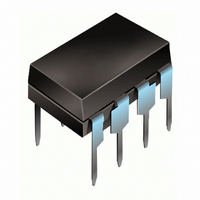
8,!! Case Outline Mechanical Specifications: Package: 8-pin DIP Tolerances: .015 (.38) unless otherwise specified Case Material: molded epoxy Weight: .07 oz. (2 gr.) WORLD HEADQUARTERS: 233 Kansas St., El Segundo, California 90245 Tel: (310) 252-7105 http://www.irf.com/ ...

Related keywords