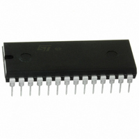
TDA7318 STMicroelectronics, TDA7318 Datasheet

TDA7318
Specifications of TDA7318
Available stocks
Related parts for TDA7318
TDA7318 Summary of contents
Page 1
... INDEPENDENT MUTE FUNCTION ALL FUNCTIONS PROGRAMMABLE VIA SE- 2 RIAL I C BUS DESCRIPTION The TDA7318 is a volume, tone (bass and treble) balance (Left/Right) and fader (front/rear) processor for quality audio applications in car radio and Hi-Fi systems. PIN CONNECTION (Top view) November 1999 FOR EXTERNAL Selectable input gain is provided ...
Page 2
... TDA7318 TEST CIRCUIT THERMAL DATA Symbol R Thermal Resistance Junction-pins th j-pins ABSOLUTE MAXIMUM RATINGS Symbol V Operating Supply Voltage S T Operating Ambient Temperature amb T Storage Temperature Range stg QUICK REFERENCE DATA Symbol V Supply Voltage S V Max. input signal handling CL THD Total Harmonic Distortion V = 1Vrms f = 1KHz ...
Page 3
... BLOCK DIAGRAM TDA7318 3/14 ...
Page 4
... TDA7318 ELECTRICAL CHARACTERISTICS (refer to the test circuit 600 , all controls flat ( 1KHz unless otherwise specified) G Symbol Parameter SUPPLY V Supply Voltage S I Supply Current S SVR Ripple Rejection INPUT SELECTORS R Input Resistance II V Clipping Level CL S Input Separation ( Output Load resistance L G Min. Input Gain ...
Page 5
... BW = 20-20KHz, flat output muted all gains = 0dB A curve all gains = 0dB all gains = 0dB 1Vrms 1Vrms -20dB V = 1Vrms 0.3Vrms -20dB V - 1.6mA O Figure 2: Signal to Noise Ratio vs. Volume Setting TDA7318 Min. Typ. Max. Unit 2 2.5 Vrms 120 4.2 4.5 4 106 dB 0.01 ...
Page 6
... TDA7318 Figure 3: Distortion & Noise vs. Frequency Figure 5: Distortion vs. Load Resistance Figure 7: Input Separation (L1 Frequency 6/14 Figure 4: Distortion & Noise vs. Frequency Figure 6: Channel Separation (L L2, L3, L4) vs. Figure 8: Supply Voltage Rejection vs. R) vs. Frequency Frequency ...
Page 7
... Figure 9: Output Clipping Level vs. Supply Voltage Figure 11: Supply Current vs. Temperature Figure 13: Typical Tone Response (with the ext. components indicated in the test circuit) Figure 10: Quiescent Current vs. Supply Voltage Figure 12: Bass Resistance vs. Temperature TDA7318 7/14 ...
Page 8
... TDA7318 BUS INTERFACE Data transmission from microprocessor to the TDA7318 and viceversa takes place thru the 2 2 wires I C BUS interface, consisting of the two lines SDA and SCL (pull-up resistors to positive supply voltage must be connected). Data Validity As shown in fig. 14, the data on the SDA line must be stable during the high period of the clock ...
Page 9
... SOFTWARE SPECIFICATION Interface Protocol The interface protocol comprises: A start condition (s) A chip address byte, containing the TDA7318 TDA7318 ADDRESS MSB first byte ACK = Acknowledge S = Start P = Stop MAX CLOCK SPEED 100kbits/s SOFTWARE SPECIFICATION Chip address MSB DATA BYTES MSB 1.25dB steps 10dB steps 2dB steps 6.25dB steps address (the 8th bit of the byte must be 0) ...
Page 10
... TDA7318 SOFTWARE SPECIFICATION (continued) DATA BYTES (detailed description) Volume MSB For example a volume of -45dB is given by Speaker Attenuators MSB For example attenuation of 25dB on speaker RF is given by 10/ LSB FUNCTION A1 A0 Volume 1.25dB steps -1. -2 -3. -6. -7 -8. Volume 10dB steps 0 -10 -20 -30 -40 -50 ...
Page 11
... For example to select the stereo 2 input with a gain of +12.5dB the 8bit string is Bass and Treble Sign For example Bass at -10dB is obtained by the following 8 bit string TDA7318 LSB FUNCTION S1 S0 Audio Switch 0 0 Stereo Stereo Stereo Stereo Not allowed 0 1 Not allowed 1 0 Not allowed 1 1 Not allowed +18.75dB +12.5dB +6.25dB 0dB ...
Page 12
... TDA7318 mm DIM. MIN. TYP. MAX. A 2.65 a1 0.1 0.3 0.004 b 0.35 0.49 0.014 b1 0.23 0.32 0.009 C 0 (typ.) D 17.7 18.1 0.697 E 10 10.65 0.394 e 1.27 e3 16.51 F 7.4 7.6 0.291 L 0.4 1.27 0.016 S 8 (max.) 12/14 inch MIN. TYP. MAX. 0.104 0.012 0.019 ...
Page 13
... DIM. MIN. TYP. MAX. MIN. a1 0.63 b 0.45 b1 0.23 0.31 0.009 b2 1.27 D 37.34 E 15.2 16.68 0.598 e 2.54 e3 33.02 F 14.1 I 4.445 L 3.3 inch MECHANICAL DATA TYP. MAX. 0.025 0.018 0.012 0.050 1.470 0.657 0.100 1.300 0.555 0.175 0.130 TDA7318 OUTLINE AND DIP28 13/14 ...
Page 14
... TDA7318 Information furnished is believed to be accurate and reliable. However, STMicroelectronics assumes no responsibility for the consequences of use of such information nor for any infringement of patents or other rights of third parties which may result from its use. No license is granted by implication or otherwise under any patent or patent rights of STMicroelectronics. Specification mentioned in this publication are subject to change without notice ...


