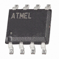
ATTINY85-20SU Atmel, ATTINY85-20SU Datasheet - Page 105

ATTINY85-20SU
Manufacturer Part Number
ATTINY85-20SU
Description
IC AVR MCU 8K 20MHZ 8SOIC
Manufacturer
Atmel
Series
AVR® ATtinyr
Specifications of ATTINY85-20SU
Core Processor
AVR
Core Size
8-Bit
Speed
20MHz
Connectivity
USI
Peripherals
Brown-out Detect/Reset, POR, PWM, WDT
Number Of I /o
6
Program Memory Size
8KB (4K x 16)
Program Memory Type
FLASH
Eeprom Size
512 x 8
Ram Size
512 x 8
Voltage - Supply (vcc/vdd)
2.7 V ~ 5.5 V
Data Converters
A/D 4x10b
Oscillator Type
Internal
Operating Temperature
-40°C ~ 85°C
Package / Case
8-SOIC (5.3mm Width), 8-SOP, 8-SOEIAJ
Processor Series
ATTINY8x
Core
AVR8
Data Bus Width
8 bit
Data Ram Size
512 B
Interface Type
USI
Maximum Clock Frequency
20 MHz
Number Of Programmable I/os
6
Number Of Timers
2
Operating Supply Voltage
2.7 V to 5.5 V
Maximum Operating Temperature
+ 85 C
Mounting Style
SMD/SMT
3rd Party Development Tools
EWAVR, EWAVR-BL
Development Tools By Supplier
ATAVRDRAGON, ATSTK500, ATSTK600, ATAVRISP2, ATAVRONEKIT
Minimum Operating Temperature
- 40 C
On-chip Adc
4-ch x 10-bit
For Use With
ATSTK600-DIP40 - STK600 SOCKET/ADAPTER 40-PDIPATAVRBC100 - REF DESIGN KIT BATTERY CHARGER770-1007 - ISP 4PORT ATMEL AVR MCU SPI/JTAG770-1004 - ISP 4PORT FOR ATMEL AVR MCU SPIATAVRDRAGON - KIT DRAGON 32KB FLASH MEM AVRATAVRISP2 - PROGRAMMER AVR IN SYSTEM
Lead Free Status / RoHS Status
Lead free / RoHS Compliant
Available stocks
Company
Part Number
Manufacturer
Quantity
Price
Part Number:
ATTINY85-20SU
Manufacturer:
ATMEL/爱特梅尔
Quantity:
20 000
- Current page: 105 of 236
- Download datasheet (5Mb)
13.3.2
13.3.3
13.3.4
2586M–AVR–07/10
GTCCR – General Timer/Counter1 Control Register
TCNT1 – Timer/Counter1
OCR1A – Timer/Counter1 Output Compare RegisterA
• Bit 2 – FOC1A: Force Output Compare Match 1A
Writing a logical one to this bit forces a change in the compare match output pin PB1 (OC1A)
according to the values already set in COM1A1 and COM1A0. If COM1A1 and COM1A0 written
in the same cycle as FOC1A, the new settings will be used. The Force Output Compare bit can
be used to change the output pin value regardless of the timer value. The automatic action pro-
grammed in COM1A1 and COM1A0 takes place as if a compare match had occurred, but no
interrupt is generated. The FOC1A bit always reads as zero. FOC1A is not in use if PWM1A bit
is set.
• Bit 1 – PSR1 : Prescaler Reset Timer/Counter1
When this bit is set (one), the Timer/Counter prescaler (TCNT1 is unaffected) will be reset. The
bit will be cleared by hardware after the operation is performed. Writing a zero to this bit will have
no effect. This bit will always read as zero.
This 8-bit register contains the value of Timer/Counter1.
Timer/Counter1 is realized as an up counter with read and write access. Due to synchronization
of the CPU, Timer/Counter1 data written into Timer/Counter1 is delayed by one CPU clock cycle
in synchronous mode and at most two CPU clock cycles for asynchronous mode.
The output compare register A is an 8-bit read/write register.
The Timer/Counter Output Compare Register A contains data to be continuously compared with
Timer/Counter1. Actions on compare matches are specified in TCCR1. A compare match does
only occur if Timer/Counter1 counts to the OCR1A value. A software write that sets TCNT1 and
OCR1A to the same value does not generate a compare match.
A compare match will set the compare interrupt flag OCF1A after a synchronization delay follow-
ing the compare event.
Bit
0x2C
Read/Write
Initial value
Bit
0x2F
Read/Write
Initial value
Bit
0x2E
Read/Write
Initial value
TSM
R/W
7
0
MSB
MSB
R/W
R/W
7
0
7
0
PWM1B
R/W
R/W
R/W
6
0
6
0
6
0
COM1B1
R/W
R/W
R/W
5
0
5
0
5
0
COM1B0
R/W
R/W
4
0
4
0
R/W
4
0
R/W
R/W
3
0
3
0
FOC1B
W
3
0
R/W
R/W
2
0
2
0
FOC1A
W
2
0
R/W
R/W
1
0
1
0
PSR1
R/W
1
0
LSB
R/W
LSB
R/W
0
0
0
0
PSR0
R/W
0
0
OCR1A
TCNT1
GTCCR
105
Related parts for ATTINY85-20SU
Image
Part Number
Description
Manufacturer
Datasheet
Request
R

Part Number:
Description:
Manufacturer:
Atmel Corporation
Datasheet:

Part Number:
Description:
Manufacturer:
Atmel Corporation
Datasheet:

Part Number:
Description:
IC MCU AVR 8K FLASH 20MHZ 20-QFN
Manufacturer:
Atmel
Datasheet:

Part Number:
Description:
IC AVR MCU 8K 20MHZ 8DIP
Manufacturer:
Atmel
Datasheet:

Part Number:
Description:
MCU AVR 8K FLASH 15MHZ 8-SOIC
Manufacturer:
Atmel
Datasheet:

Part Number:
Description:
MCU AVR 8KB FLASH 20MHZ 8SOIC
Manufacturer:
Atmel
Datasheet:

Part Number:
Description:
IC MCU AVR 8KB FLASH 20MHZ 8SOIC
Manufacturer:
Atmel
Datasheet:

Part Number:
Description:
MCU AVR 8KB FLASH 20MHZ 20QFN
Manufacturer:
Atmel
Datasheet:

Part Number:
Description:
IC AVR MCU 8K 20MHZ 8DIP
Manufacturer:
Atmel
Datasheet:

Part Number:
Description:
IC AVR MCU 8K 20MHZ 8SOIC
Manufacturer:
Atmel
Datasheet:


