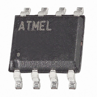
ATTINY85-20SU Atmel, ATTINY85-20SU Datasheet - Page 62

ATTINY85-20SU
Manufacturer Part Number
ATTINY85-20SU
Description
IC AVR MCU 8K 20MHZ 8SOIC
Manufacturer
Atmel
Series
AVR® ATtinyr
Specifications of ATTINY85-20SU
Core Processor
AVR
Core Size
8-Bit
Speed
20MHz
Connectivity
USI
Peripherals
Brown-out Detect/Reset, POR, PWM, WDT
Number Of I /o
6
Program Memory Size
8KB (4K x 16)
Program Memory Type
FLASH
Eeprom Size
512 x 8
Ram Size
512 x 8
Voltage - Supply (vcc/vdd)
2.7 V ~ 5.5 V
Data Converters
A/D 4x10b
Oscillator Type
Internal
Operating Temperature
-40°C ~ 85°C
Package / Case
8-SOIC (5.3mm Width), 8-SOP, 8-SOEIAJ
Processor Series
ATTINY8x
Core
AVR8
Data Bus Width
8 bit
Data Ram Size
512 B
Interface Type
USI
Maximum Clock Frequency
20 MHz
Number Of Programmable I/os
6
Number Of Timers
2
Operating Supply Voltage
2.7 V to 5.5 V
Maximum Operating Temperature
+ 85 C
Mounting Style
SMD/SMT
3rd Party Development Tools
EWAVR, EWAVR-BL
Development Tools By Supplier
ATAVRDRAGON, ATSTK500, ATSTK600, ATAVRISP2, ATAVRONEKIT
Minimum Operating Temperature
- 40 C
On-chip Adc
4-ch x 10-bit
For Use With
ATSTK600-DIP40 - STK600 SOCKET/ADAPTER 40-PDIPATAVRBC100 - REF DESIGN KIT BATTERY CHARGER770-1007 - ISP 4PORT ATMEL AVR MCU SPI/JTAG770-1004 - ISP 4PORT FOR ATMEL AVR MCU SPIATAVRDRAGON - KIT DRAGON 32KB FLASH MEM AVRATAVRISP2 - PROGRAMMER AVR IN SYSTEM
Lead Free Status / RoHS Status
Lead free / RoHS Compliant
Available stocks
Company
Part Number
Manufacturer
Quantity
Price
Part Number:
ATTINY85-20SU
Manufacturer:
ATMEL/爱特梅尔
Quantity:
20 000
- Current page: 62 of 236
- Download datasheet (5Mb)
10.3.1
62
ATtiny25/45/85
Alternate Functions of Port B
The following subsections shortly describe the alternate functions for each port, and relate the
overriding signals to the alternate function. Refer to the alternate function description for further
details.
The Port B pins with alternate function are shown in
Table 10-3.
• Port B, Bit 5 – RESET/dW/ADC0/PCINT5
• RESET: External Reset input is active low and enabled by unprogramming (“1”) the
• dW: When the debugWIRE Enable (DWEN) Fuse is programmed and Lock bits are
RSTDISBL Fuse. Pullup is activated and output driver and digital input are deactivated when
the pin is used as the RESET pin.
unprogrammed, the debugWIRE system within the target device is activated. The RESET
Port Pin
PB5
PB4
PB3
PB2
PB1
PB0
Port B Pins Alternate Functions
Alternate Function
RESET: Reset Pin
dW:
ADC0:
PCINT5: Pin Change Interrupt, Source 5
XTAL2: Crystal Oscillator Output
CLKO: System Clock Output
ADC2:
OC1B: Timer/Counter1 Compare Match B Output
PCINT4: Pin Change Interrupt 0, Source 4
XTAL1: Crystal Oscillator Input
CLKI:
ADC3:
OC1B: Complementary Timer/Counter1 Compare Match B Output
PCINT3: Pin Change Interrupt 0, Source 3
SCK:
ADC1:
T0:
USCK: USI Clock (Three Wire Mode)
SCL :
INT0:
PCINT2: Pin Change Interrupt 0, Source 2
MISO:
AIN1:
OC0B: Timer/Counter0 Compare Match B Output
OC1A: Timer/Counter1 Compare Match A Output
DO:
PCINT1:Pin Change Interrupt 0, Source 1
MOSI:: SPI Master Data Output / Slave Data Input
AIN0:
OC0A: Timer/Counter0 Compare Match A output
OC1A: Complementary Timer/Counter1 Compare Match A Output
DI:
SDA:
AREF:
PCINT0: Pin Change Interrupt 0, Source 0
debugWIRE I/O
ADC Input Channel 0
ADC Input Channel 2
External Clock Input
ADC Input Channel 3
Serial Clock Input
ADC Input Channel 1
Timer/Counter0 Clock Source
USI Clock (Two Wire Mode)
External Interrupt 0 Input
SPI Master Data Input / Slave Data Output
Analog Comparator, Negative Input
USI Data Output (Three Wire Mode)
Analog Comparator, Positive Input
USI Data Input (Three Wire Mode)
USI Data Input (Two Wire Mode)
External Analog Reference
Table
10-3.
2586M–AVR–07/10
Related parts for ATTINY85-20SU
Image
Part Number
Description
Manufacturer
Datasheet
Request
R

Part Number:
Description:
Manufacturer:
Atmel Corporation
Datasheet:

Part Number:
Description:
Manufacturer:
Atmel Corporation
Datasheet:

Part Number:
Description:
IC MCU AVR 8K FLASH 20MHZ 20-QFN
Manufacturer:
Atmel
Datasheet:

Part Number:
Description:
IC AVR MCU 8K 20MHZ 8DIP
Manufacturer:
Atmel
Datasheet:

Part Number:
Description:
MCU AVR 8K FLASH 15MHZ 8-SOIC
Manufacturer:
Atmel
Datasheet:

Part Number:
Description:
MCU AVR 8KB FLASH 20MHZ 8SOIC
Manufacturer:
Atmel
Datasheet:

Part Number:
Description:
IC MCU AVR 8KB FLASH 20MHZ 8SOIC
Manufacturer:
Atmel
Datasheet:

Part Number:
Description:
MCU AVR 8KB FLASH 20MHZ 20QFN
Manufacturer:
Atmel
Datasheet:

Part Number:
Description:
IC AVR MCU 8K 20MHZ 8DIP
Manufacturer:
Atmel
Datasheet:

Part Number:
Description:
IC AVR MCU 8K 20MHZ 8SOIC
Manufacturer:
Atmel
Datasheet:


