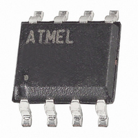
ATTINY85-20SU Atmel, ATTINY85-20SU Datasheet - Page 63

ATTINY85-20SU
Manufacturer Part Number
ATTINY85-20SU
Description
IC AVR MCU 8K 20MHZ 8SOIC
Manufacturer
Atmel
Series
AVR® ATtinyr
Specifications of ATTINY85-20SU
Core Processor
AVR
Core Size
8-Bit
Speed
20MHz
Connectivity
USI
Peripherals
Brown-out Detect/Reset, POR, PWM, WDT
Number Of I /o
6
Program Memory Size
8KB (4K x 16)
Program Memory Type
FLASH
Eeprom Size
512 x 8
Ram Size
512 x 8
Voltage - Supply (vcc/vdd)
2.7 V ~ 5.5 V
Data Converters
A/D 4x10b
Oscillator Type
Internal
Operating Temperature
-40°C ~ 85°C
Package / Case
8-SOIC (5.3mm Width), 8-SOP, 8-SOEIAJ
Processor Series
ATTINY8x
Core
AVR8
Data Bus Width
8 bit
Data Ram Size
512 B
Interface Type
USI
Maximum Clock Frequency
20 MHz
Number Of Programmable I/os
6
Number Of Timers
2
Operating Supply Voltage
2.7 V to 5.5 V
Maximum Operating Temperature
+ 85 C
Mounting Style
SMD/SMT
3rd Party Development Tools
EWAVR, EWAVR-BL
Development Tools By Supplier
ATAVRDRAGON, ATSTK500, ATSTK600, ATAVRISP2, ATAVRONEKIT
Minimum Operating Temperature
- 40 C
On-chip Adc
4-ch x 10-bit
For Use With
ATSTK600-DIP40 - STK600 SOCKET/ADAPTER 40-PDIPATAVRBC100 - REF DESIGN KIT BATTERY CHARGER770-1007 - ISP 4PORT ATMEL AVR MCU SPI/JTAG770-1004 - ISP 4PORT FOR ATMEL AVR MCU SPIATAVRDRAGON - KIT DRAGON 32KB FLASH MEM AVRATAVRISP2 - PROGRAMMER AVR IN SYSTEM
Lead Free Status / RoHS Status
Lead free / RoHS Compliant
Available stocks
Company
Part Number
Manufacturer
Quantity
Price
Part Number:
ATTINY85-20SU
Manufacturer:
ATMEL/爱特梅尔
Quantity:
20 000
- Current page: 63 of 236
- Download datasheet (5Mb)
2586M–AVR–07/10
• Port B, Bit 4 – XTAL2/CLKO/ADC2/OC1B/PCINT4
• Port B, Bit 3 – XTAL1/CLKI/ADC3/OC1B/PCINT3
• Port B, Bit 2 – SCK/ADC1/T0/USCK/SCL/INT0/PCINT2
• Port B, Bit 1 – MISO/AIN1/OC0B/OC1A/DO/PCINT1
• ADC0: Analog to Digital Converter, Channel 0
• PCINT5: Pin Change Interrupt source 5.
• XTAL2: Chip Clock Oscillator pin 2. Used as clock pin for all chip clock sources except
• CLKO: The devided system clock can be output on the pin PB4. The divided system clock
• ADC2: Analog to Digital Converter, Channel 2
• OC1B: Output Compare Match output: The PB4 pin can serve as an external output for the
• PCINT4: Pin Change Interrupt source 4.
• XTAL1: Chip Clock Oscillator pin 1. Used for all chip clock sources except internal
• CLKI: Clock Input from an external clock source, see
• ADC3: Analog to Digital Converter, Channel 3
• OC1B: Inverted Output Compare Match output: The PB3 pin can serve as an external output
• PCINT3: Pin Change Interrupt source 3.
• SCK: Master Clock output, Slave Clock input pin for SPI channel. When the SPI is enabled
• ADC1: Analog to Digital Converter, Channel 1
• T0: Timer/Counter0 counter source.
• USCK: Three-wire mode Universal Serial Interface Clock.
• SCL: Two-wire mode Serial Clock for USI Two-wire mode.
• INT0: External Interrupt source 0.
• PCINT2: Pin Change Interrupt source 2.
• MISO: Master Data input, Slave Data output pin for SPI channel. When the SPI is enabled as
port pin is configured as a wire-AND (open-drain) bi-directional I/O pin with pull-up enabled
and becomes the communication gateway between target and emulator.
internal calibrateble RC Oscillator and external clock. When used as a clock pin, the pin can
not be used as an I/O pin. When using internal calibratable RC Oscillator or External clock as
a Chip clock sources, PB4 serves as an ordinary I/O pin.
will be output if the CKOUT Fuse is programmed, regardless of the PORTB4 and DDB4
settings. It will also be output during reset.
Timer/Counter1 Compare Match B when configured as an output (DDB4 set). The OC1B pin
is also the output pin for the PWM mode timer function.
calibrateble RC oscillator. When used as a clock pin, the pin can not be used as an I/O pin.
for the Timer/Counter1 Compare Match B when configured as an output (DDB3 set). The
OC1B pin is also the inverted output pin for the PWM mode timer function.
as a Slave, this pin is configured as an input regardless of the setting of DDB2. When the SPI
is enabled as a Master, the data direction of this pin is controlled by DDPB2. When the pin is
forced by the SPI to be an input, the pull-up can still be controlled by the PORTB2 bit.
a Master, this pin is configured as an input regardless of the setting of DDB1. When the SPI
is enabled as a Slave, the data direction of this pin is controlled by DDB1. When the pin is
forced by the SPI to be an input, the pull-up can still be controlled by the PORTB1 bit.
.
.
.
.
“External Clock” on page
26.
63
Related parts for ATTINY85-20SU
Image
Part Number
Description
Manufacturer
Datasheet
Request
R

Part Number:
Description:
Manufacturer:
Atmel Corporation
Datasheet:

Part Number:
Description:
Manufacturer:
Atmel Corporation
Datasheet:

Part Number:
Description:
IC MCU AVR 8K FLASH 20MHZ 20-QFN
Manufacturer:
Atmel
Datasheet:

Part Number:
Description:
IC AVR MCU 8K 20MHZ 8DIP
Manufacturer:
Atmel
Datasheet:

Part Number:
Description:
MCU AVR 8K FLASH 15MHZ 8-SOIC
Manufacturer:
Atmel
Datasheet:

Part Number:
Description:
MCU AVR 8KB FLASH 20MHZ 8SOIC
Manufacturer:
Atmel
Datasheet:

Part Number:
Description:
IC MCU AVR 8KB FLASH 20MHZ 8SOIC
Manufacturer:
Atmel
Datasheet:

Part Number:
Description:
MCU AVR 8KB FLASH 20MHZ 20QFN
Manufacturer:
Atmel
Datasheet:

Part Number:
Description:
IC AVR MCU 8K 20MHZ 8DIP
Manufacturer:
Atmel
Datasheet:

Part Number:
Description:
IC AVR MCU 8K 20MHZ 8SOIC
Manufacturer:
Atmel
Datasheet:


