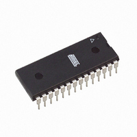
ATMEGA48-20PU Atmel, ATMEGA48-20PU Datasheet - Page 259

ATMEGA48-20PU
Manufacturer Part Number
ATMEGA48-20PU
Description
IC AVR MCU 4K 20MHZ 5V 28DIP
Manufacturer
Atmel
Series
AVR® ATmegar
Datasheets
1.ATAVRTS2080B.pdf
(378 pages)
2.ATMEGA48-20AU.pdf
(35 pages)
3.ATMEGA48-20PU.pdf
(377 pages)
Specifications of ATMEGA48-20PU
Core Processor
AVR
Core Size
8-Bit
Speed
20MHz
Connectivity
I²C, SPI, UART/USART
Peripherals
Brown-out Detect/Reset, POR, PWM, WDT
Number Of I /o
23
Program Memory Size
4KB (2K x 16)
Program Memory Type
FLASH
Eeprom Size
256 x 8
Ram Size
512 x 8
Voltage - Supply (vcc/vdd)
2.7 V ~ 5.5 V
Data Converters
A/D 6x10b
Oscillator Type
Internal
Operating Temperature
-40°C ~ 85°C
Package / Case
28-DIP (0.300", 7.62mm)
Processor Series
ATMEGA48x
Core
AVR8
Data Bus Width
8 bit
Data Ram Size
512 B
Interface Type
2-Wire/SPI/USART/Serial
Maximum Clock Frequency
20 MHz
Number Of Programmable I/os
23
Number Of Timers
3
Operating Supply Voltage
2.7 V to 5.5 V
Maximum Operating Temperature
+ 85 C
Mounting Style
Through Hole
3rd Party Development Tools
EWAVR, EWAVR-BL
Development Tools By Supplier
ATAVRDRAGON, ATSTK500, ATSTK600, ATAVRISP2, ATAVRONEKIT
Minimum Operating Temperature
- 40 C
On-chip Adc
6-ch x 10-bit
Cpu Family
ATmega
Device Core
AVR
Device Core Size
8b
Frequency (max)
20MHz
Total Internal Ram Size
512Byte
# I/os (max)
23
Number Of Timers - General Purpose
3
Operating Supply Voltage (typ)
3.3/5V
Operating Supply Voltage (max)
5.5V
Operating Supply Voltage (min)
2.7V
Instruction Set Architecture
RISC
Operating Temp Range
-40C to 85C
Operating Temperature Classification
Industrial
Mounting
Through Hole
Pin Count
28
Package Type
PDIP
For Use With
ATSTK600-TQFP32 - STK600 SOCKET/ADAPTER 32-TQFPATSTK600 - DEV KIT FOR AVR/AVR32770-1007 - ISP 4PORT ATMEL AVR MCU SPI/JTAGATAVRDRAGON - KIT DRAGON 32KB FLASH MEM AVRATAVRISP2 - PROGRAMMER AVR IN SYSTEMATJTAGICE2 - AVR ON-CHIP D-BUG SYSTEM
Lead Free Status / RoHS Status
Lead free / RoHS Compliant
- Current page: 259 of 378
- Download datasheet (8Mb)
24. debugWIRE On-chip Debug System
24.1
24.2
24.3
2545S–AVR–07/10
Features
Overview
Physical Interface
•
•
•
•
•
•
•
•
•
•
The debugWIRE On-chip debug system uses a One-wire, bi-directional interface to control the
program flow, execute AVR instructions in the CPU and to program the different non-volatile
memories.
When the debugWIRE Enable (DWEN) Fuse is programmed and Lock bits are unprogrammed,
the debugWIRE system within the target device is activated. The RESET port pin is configured
as a wire-AND (open-drain) bi-directional I/O pin with pull-up enabled and becomes the commu-
nication gateway between target and emulator.
Figure 24-1. The debugWIRE Setup
Figure 24-1
connector. The system clock is not affected by debugWIRE and will always be the clock source
selected by the CKSEL Fuses.
Complete Program Flow Control
Emulates All On-chip Functions, Both Digital and Analog, except RESET Pin
Real-time Operation
Symbolic Debugging Support (Both at C and Assembler Source Level, or for Other HLLs)
Unlimited Number of Program Break Points (Using Software Break Points)
Non-intrusive Operation
Electrical Characteristics Identical to Real Device
Automatic Configuration System
High-Speed Operation
Programming of Non-volatile Memories
shows the schematic of a target MCU, with debugWIRE enabled, and the emulator
dW
GND
dW(RESET)
VCC
ATmega48/88/168
1.8 - 5.5V
259
Related parts for ATMEGA48-20PU
Image
Part Number
Description
Manufacturer
Datasheet
Request
R

Part Number:
Description:
IC AVR MCU 4K 5V 20MHZ 32-TQFP
Manufacturer:
Atmel
Datasheet:

Part Number:
Description:
Manufacturer:
Atmel Corporation
Datasheet:

Part Number:
Description:
Manufacturer:
Atmel Corporation
Datasheet:

Part Number:
Description:
IC AVR MCU 4K 20MHZ 5V 32TQFP
Manufacturer:
Atmel
Datasheet:

Part Number:
Description:
IC AVR MCU 4K 20MHZ 5V 32-QFN
Manufacturer:
Atmel
Datasheet:

Part Number:
Description:
IC AVR MCU 4K 5V 20MHZ 32-TQFP
Manufacturer:
Atmel
Datasheet:

Part Number:
Description:
IC AVR MCU 4K 5V 20MHZ 32-QFN
Manufacturer:
Atmel
Datasheet:

Part Number:
Description:
IC AVR MCU 4K 5V 20MHZ 32-QFN
Manufacturer:
Atmel
Datasheet:

Part Number:
Description:
IC AVR MCU 4K 5V 20MHZ 28-DIP
Manufacturer:
Atmel
Datasheet:

Part Number:
Description:
IC AVR MCU 4K 5V 20MHZ 28-DIP
Manufacturer:
Atmel
Datasheet:

Part Number:
Description:
IC AVR MCU 4K FLASH 20MHZ 28QFN
Manufacturer:
Atmel
Datasheet:

Part Number:
Description:
MCU AVR 4KB FLASH 20MHZ 32QFN
Manufacturer:
Atmel
Datasheet:


