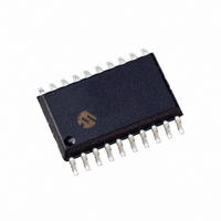
DSPIC33FJ12MC201-I/SO Microchip Technology, DSPIC33FJ12MC201-I/SO Datasheet - Page 81

DSPIC33FJ12MC201-I/SO
Manufacturer Part Number
DSPIC33FJ12MC201-I/SO
Description
IC DSPIC MCU/DSP 12K 20SOIC
Manufacturer
Microchip Technology
Series
dsPIC™ 33Fr
Datasheets
1.PIC24HJ12GP201-ISO.pdf
(84 pages)
2.DSPIC33FJ12MC201-ISO.pdf
(288 pages)
3.DSPIC33FJ12MC201-ISO.pdf
(14 pages)
4.DSPIC33FJ12MC201-IP.pdf
(284 pages)
Specifications of DSPIC33FJ12MC201-I/SO
Program Memory Type
FLASH
Program Memory Size
12KB (12K x 8)
Package / Case
20-SOIC (7.5mm Width)
Core Processor
dsPIC
Core Size
16-Bit
Speed
40 MIPs
Connectivity
I²C, IrDA, SPI, UART/USART
Peripherals
Brown-out Detect/Reset, Motor Control PWM, QEI, POR, PWM, WDT
Number Of I /o
15
Ram Size
1K x 8
Voltage - Supply (vcc/vdd)
3 V ~ 3.6 V
Data Converters
A/D 4x10b
Oscillator Type
Internal
Operating Temperature
-40°C ~ 85°C
Product
DSCs
Data Bus Width
16 bit
Processor Series
DSPIC33F
Core
dsPIC
Maximum Clock Frequency
40 MHz
Number Of Programmable I/os
15
Data Ram Size
1 KB
Maximum Operating Temperature
+ 85 C
Mounting Style
SMD/SMT
3rd Party Development Tools
52713-733, 52714-737, 53276-922, EWDSPIC
Development Tools By Supplier
PG164130, DV164035, DV244005, DV164005, PG164120, DM240001, DV164033
Minimum Operating Temperature
- 40 C
Lead Free Status / RoHS Status
Lead free / RoHS Compliant
For Use With
DV164033 - KIT START EXPLORER 16 MPLAB ICD2DM240001 - BOARD DEMO PIC24/DSPIC33/PIC32
Eeprom Size
-
Lead Free Status / Rohs Status
Lead free / RoHS Compliant
Revision G (March 2009) (Continued)
• Removed PROGW and renamed QBLANK to
• Updated the flowchart in
• Updated the second paragraph in
• Changed the CFGB calculation for
• Removed Note 2 in
• Updated the Erased Value and Value with
• Removed COE and BKBUG Configuration Bit
• Added PLLKEN to FWDT in
• Added ALTQIO and ALTSS1 to FPOR in
© 2010 Microchip Technology Inc.
QBLANKEX in the Command Set Summary, and
added the following commands (see
- ERASEB
- ERASEP
- CRCP
“Confirming the Presence of the Programming
Executive”
dsPIC33FJ06GS101/102/202 and
dsPIC33FJ16GS402/404/502/504 devices to:
+ (FPOR & 0x0F)
0xAAAAAA at 0x0 and Last Code Address
columns in Table 3-2 for the following devices:
- dsPIC33FJ64GP202
- dsPIC33FJ64GP204
- dsPIC33FJ64GP802
- dsPIC33FJ64GP804
- dsPIC33FJ64MC202
- dsPIC33FJ64MC204
- dsPIC33FJ64MC802
- dsPIC33FJ64MC804
- PIC24HJ64GP202
- PIC24HJ64GP204
- PIC24HJ64GP502
- PIC24HJ64GP504
Descriptions in
Table 3-3
Table 3-2
and Table 3-3
Table 3-2
Section 3.6.1 “Overview”
Figure 3-2
and Table 3-3
Table 3-2
Section 3.2
Table
and
3-1):
• Removed Notes for the following Configuration Bit
• Added Note 6 and Note 7 to Table 3-3
• Added Note 1 to
• Added Note to the beginning of
• Updated the third paragraph in
• Changed the clock speed to be provided by the
• Added
• Removed FUID2 and FUID3 from
• Added new Default Configuration Register Value
• Updated description for FWDT and added Note 1
• Added seven new op code instructions to Step 3
• Updated Step 4 in
• Added new columns (Application ID and JTAG ID)
• Added JTAG Type registers (see
• The following updates were made to
Descriptions in
- RBS
- RSS (removed Note 1)
- SSS
- SWRP
- IOL1WAY
- ALTI2C
- BOREN
Programming Executive”
“Communication Interface and Protocol”
clarify the clock response time
programmer from 7.35 MHz to 1.85 MHz in
Section 4.1.2 “SPI Rate”
(formerly Figure 5-2)
table in support of dsPIC33FJ32GSX06/60X/610
and dsPIC33FJ64GSX06/60X/610 devices (see
Table
in
in
pointer increment
to
Register 7-2
- Updated parameters P1A and P1B and
- Updated characteristic for parameter P16
- Updated minimum value and units for
- Added new parameter P21
added additional characteristics and values
parameter P18
Table 5-10
Table 6-1
Table 7-1
5-9)
Figure 5-2
and
Table
Figure 3-5
Register
and updated
Table 6-1
3-2:
7-3)
to reflect the TBLPG
Section 4.1.1
Figure 5-3
Section 4.0 “The
Register
DS70152H-page 81
Table 5-6
Table 8-1
7-1,
to


