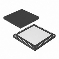
DSPIC33FJ128GP206A-I/MR Microchip Technology, DSPIC33FJ128GP206A-I/MR Datasheet - Page 173

DSPIC33FJ128GP206A-I/MR
Manufacturer Part Number
DSPIC33FJ128GP206A-I/MR
Description
IC DSPIC MCU/DSP 128K 64-QFN
Manufacturer
Microchip Technology
Series
dsPIC™ 33Fr
Datasheet
1.DSPIC33FJ64GP206A-IMR.pdf
(338 pages)
Specifications of DSPIC33FJ128GP206A-I/MR
Core Processor
dsPIC
Core Size
16-Bit
Speed
40 MIPs
Connectivity
I²C, IrDA, LIN, SPI, UART/USART
Peripherals
AC'97, Brown-out Detect/Reset, DMA, I²S, POR, PWM, WDT
Number Of I /o
53
Program Memory Size
128KB (128K x 8)
Program Memory Type
FLASH
Ram Size
8K x 8
Voltage - Supply (vcc/vdd)
3 V ~ 3.6 V
Data Converters
A/D 18x10b/12b
Oscillator Type
Internal
Operating Temperature
-40°C ~ 85°C
Package / Case
64-VFQFN, Exposed Pad
Product
DSCs
Processor Series
DSPIC33F
Core
dsPIC
3rd Party Development Tools
52713-733, 52714-737, 53276-922, EWDSPIC
Development Tools By Supplier
PG164130, DV164035, DV244005, DV164005, PG164120, DM240001, DV164033
Lead Free Status / RoHS Status
Lead free / RoHS Compliant
Eeprom Size
-
Lead Free Status / Rohs Status
Lead free / RoHS Compliant
- Current page: 173 of 338
- Download datasheet (3Mb)
REGISTER 13-2:
2009 Microchip Technology Inc.
bit 15
bit 7
Legend:
R = Readable bit
-n = Value at POR
bit 15
bit 14
bit 13
bit 12-7
bit 6
bit 5-4
bit 3-2
bit 1
bit 0
Note 1: When 32-bit operation is enabled (T2CON<3> = 1), these bits have no effect on Timery operation; all timer
TON
R/W-0
U-0
—
2: When 32-bit timer operation is enabled (T32 = 1) in the Timer Control register (TxCON<3>), the TSIDL bit
3: The TyCK pin is not available on all timers. Refer to the “Pin Diagrams” section for the available pins.
(1)
functions are set through T2CON.
must be cleared to operate the 32-bit timer in Idle mode.
TON: Timery On bit
1 = Starts 16-bit Timery
0 = Stops 16-bit Timery
Unimplemented: Read as ‘0’
TSIDL: Stop in Idle Mode bit
1 = Discontinue module operation when device enters Idle mode
0 = Continue module operation in Idle mode
Unimplemented: Read as ‘0’
TGATE: Timery Gated Time Accumulation Enable bit
When TCS = 1:
This bit is ignored.
When TCS = 0:
1 = Gated time accumulation enabled
0 = Gated time accumulation disabled
TCKPS<1:0>: Timer3 Input Clock Prescale Select bits
11 = 1:256
10 = 1:64
01 = 1:8
00 = 1:1
Unimplemented: Read as ‘0’
TCS: Timery Clock Source Select bit
1 = External clock from pin TyCK (on the rising edge)
0 = Internal clock (F
Unimplemented: Read as ‘0’
TGATE
R/W-0
U-0
—
TyCON (T3CON, T5CON, T7CON OR T9CON) CONTROL REGISTER
(1)
dsPIC33FJXXXGPX06A/X08A/X10A
W = Writable bit
‘1’ = Bit is set
TSIDL
R/W-0
R/W-0
(1)
CY
TCKPS<1:0>
)
(2)
(2)
R/W-0
U-0
(1)
Preliminary
—
(1,3)
U = Unimplemented bit, read as ‘0’
‘0’ = Bit is cleared
U-0
U-0
—
—
(1)
(1)
U-0
U-0
—
—
x = Bit is unknown
TCS
R/W-0
U-0
—
(1,3)
DS70593B-page 173
U-0
U-0
—
—
bit 8
bit 0
Related parts for DSPIC33FJ128GP206A-I/MR
Image
Part Number
Description
Manufacturer
Datasheet
Request
R

Part Number:
Description:
Manufacturer:
Microchip Technology Inc.
Datasheet:

Part Number:
Description:
Manufacturer:
Microchip Technology Inc.
Datasheet:

Part Number:
Description:
Manufacturer:
Microchip Technology Inc.
Datasheet:

Part Number:
Description:
Manufacturer:
Microchip Technology Inc.
Datasheet:

Part Number:
Description:
Manufacturer:
Microchip Technology Inc.
Datasheet:

Part Number:
Description:
Manufacturer:
Microchip Technology Inc.
Datasheet:

Part Number:
Description:
Manufacturer:
Microchip Technology Inc.
Datasheet:

Part Number:
Description:
Manufacturer:
Microchip Technology Inc.
Datasheet:


