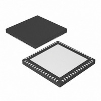
DSPIC33FJ128GP206A-I/MR Microchip Technology, DSPIC33FJ128GP206A-I/MR Datasheet - Page 246

DSPIC33FJ128GP206A-I/MR
Manufacturer Part Number
DSPIC33FJ128GP206A-I/MR
Description
IC DSPIC MCU/DSP 128K 64-QFN
Manufacturer
Microchip Technology
Series
dsPIC™ 33Fr
Datasheet
1.DSPIC33FJ64GP206A-IMR.pdf
(338 pages)
Specifications of DSPIC33FJ128GP206A-I/MR
Core Processor
dsPIC
Core Size
16-Bit
Speed
40 MIPs
Connectivity
I²C, IrDA, LIN, SPI, UART/USART
Peripherals
AC'97, Brown-out Detect/Reset, DMA, I²S, POR, PWM, WDT
Number Of I /o
53
Program Memory Size
128KB (128K x 8)
Program Memory Type
FLASH
Ram Size
8K x 8
Voltage - Supply (vcc/vdd)
3 V ~ 3.6 V
Data Converters
A/D 18x10b/12b
Oscillator Type
Internal
Operating Temperature
-40°C ~ 85°C
Package / Case
64-VFQFN, Exposed Pad
Product
DSCs
Processor Series
DSPIC33F
Core
dsPIC
3rd Party Development Tools
52713-733, 52714-737, 53276-922, EWDSPIC
Development Tools By Supplier
PG164130, DV164035, DV244005, DV164005, PG164120, DM240001, DV164033
Lead Free Status / RoHS Status
Lead free / RoHS Compliant
Eeprom Size
-
Lead Free Status / Rohs Status
Lead free / RoHS Compliant
- Current page: 246 of 338
- Download datasheet (3Mb)
dsPIC33FJXXXGPX06A/X08A/X10A
REGISTER 21-9:
REGISTER 21-10: ADxPCFGL: ADCx PORT CONFIGURATION REGISTER LOW
DS70593B-page 246
bit 15
bit 7
Legend:
R = Readable bit
-n = Value at POR
bit 15-0
bit 15
bit 7
Legend:
R = Readable bit
-n = Value at POR
bit 15-0
Note 1: On devices without 32 analog inputs, all PCFG bits are R/W by user. However, PCFG bits are ignored on
Note 1: On devices without 16 analog inputs, all PCFG bits are R/W by user. However, PCFG bits are ignored on
PCFG31
PCFG23
PCFG15
PCFG7
R/W-0
R/W-0
R/W-0
R/W-0
2: ADC2 only supports analog inputs AN0-AN15; therefore, no ADC2 port Configuration register exists.
3: PCFGx = ANx, where x = 16 through 31.
4: PCFGx bits have no effect if ADC module is disabled by setting ADxMD bit in the PMDx register. In this
2: On devices with two analog-to-digital modules, both AD1PCFGL and AD2PCFGL will affect the
3: PCFGx = ANx, where x = 0 through 15.
4: PCFGx bits have no effect if ADC module is disabled by setting ADxMD bit in the PMDx register. In this
ports without a corresponding input on device.
case all port pins multiplexed with ANx will be in Digital mode.
ports without a corresponding input on device.
configuration of port pins multiplexed with AN0-AN15.
case all port pins multiplexed with ANx will be in Digital mode
PCFG<31:16>: ADC Port Configuration Control bits
1 = Port pin in Digital mode, port read input enabled, ADC input multiplexer connected to AV
0 = Port pin in Analog mode, port read input disabled, ADC samples pin voltage
PCFG<15:0>: ADC Port Configuration Control bits
1 = Port pin in Digital mode, port read input enabled, ADC input multiplexer connected to AV
0 = Port pin in Analog mode, port read input disabled, ADC samples pin voltage
PCFG30
PCFG22
PCFG14
PCFG6
R/W-0
R/W-0
R/W-0
R/W-0
AD1PCFGH: ADC1 PORT CONFIGURATION REGISTER HIGH
W = Writable bit
‘1’ = Bit is set
W = Writable bit
‘1’ = Bit is set
PCFG29
PCFG21
PCFG13
PCFG5
R/W-0
R/W-0
R/W-0
R/W-0
PCFG28
PCFG20
PCFG12
PCFG4
R/W-0
R/W-0
R/W-0
R/W-0
Preliminary
U = Unimplemented bit, read as ‘0’
‘0’ = Bit is cleared
U = Unimplemented bit, read as ‘0’
‘0’ = Bit is cleared
PCFG27
PCFG19
PCFG11
PCFG3
R/W-0
R/W-0
R/W-0
R/W-0
PCFG26
PCFG18
PCFG10
PCFG2
R/W-0
R/W-0
R/W-0
R/W-0
2009 Microchip Technology Inc.
x = Bit is unknown
x = Bit is unknown
PCFG25
PCFG17
PCFG9
PCFG1
R/W-0
R/W-0
R/W-0
R/W-0
(1,2,3,4)
(1,2,3,4)
PCFG24
PCFG16
PCFG8
PCFG0
R/W-0
R/W-0
R/W-0
R/W-0
SS
SS
bit 8
bit 0
bit 8
bit 0
Related parts for DSPIC33FJ128GP206A-I/MR
Image
Part Number
Description
Manufacturer
Datasheet
Request
R

Part Number:
Description:
Manufacturer:
Microchip Technology Inc.
Datasheet:

Part Number:
Description:
Manufacturer:
Microchip Technology Inc.
Datasheet:

Part Number:
Description:
Manufacturer:
Microchip Technology Inc.
Datasheet:

Part Number:
Description:
Manufacturer:
Microchip Technology Inc.
Datasheet:

Part Number:
Description:
Manufacturer:
Microchip Technology Inc.
Datasheet:

Part Number:
Description:
Manufacturer:
Microchip Technology Inc.
Datasheet:

Part Number:
Description:
Manufacturer:
Microchip Technology Inc.
Datasheet:

Part Number:
Description:
Manufacturer:
Microchip Technology Inc.
Datasheet:


