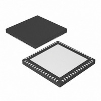
DSPIC33FJ128MC506A-I/MR Microchip Technology, DSPIC33FJ128MC506A-I/MR Datasheet - Page 199

DSPIC33FJ128MC506A-I/MR
Manufacturer Part Number
DSPIC33FJ128MC506A-I/MR
Description
IC DSPIC MCU/DSP 128K 64-QFN
Manufacturer
Microchip Technology
Series
dsPIC™ 33Fr
Datasheet
1.DSPIC33FJ64MC506A-IPT.pdf
(352 pages)
Specifications of DSPIC33FJ128MC506A-I/MR
Core Processor
dsPIC
Core Size
16-Bit
Speed
40 MIPs
Connectivity
CAN, I²C, IrDA, LIN, SPI, UART/USART
Peripherals
Brown-out Detect/Reset, DMA, Motor Control PWM, QEI, POR, PWM, WDT
Number Of I /o
53
Program Memory Size
128KB (128K x 8)
Program Memory Type
FLASH
Ram Size
8K x 8
Voltage - Supply (vcc/vdd)
3 V ~ 3.6 V
Data Converters
A/D 16x10b/12b
Oscillator Type
Internal
Operating Temperature
-40°C ~ 85°C
Package / Case
64-VFQFN, Exposed Pad
Product
DSCs
Processor Series
DSPIC33F
Core
dsPIC
3rd Party Development Tools
52713-733, 52714-737, 53276-922, EWDSPIC
Development Tools By Supplier
PG164130, DV164035, DV244005, DV164005, PG164120, DM240001, DV164033
Lead Free Status / RoHS Status
Lead free / RoHS Compliant
Eeprom Size
-
Lead Free Status / Rohs Status
Lead free / RoHS Compliant
- Current page: 199 of 352
- Download datasheet (3Mb)
REGISTER 18-2:
2009 Microchip Technology Inc.
bit 15
bit 7
Legend:
R = Readable bit
-n = Value at POR
bit 15-13
bit 12
bit 11
bit 10
bit 9
bit 8
bit 7
bit 6
bit 5
Note 1:
SSEN
R/W-0
U-0
—
2:
3:
(3)
The CKE bit is not used in the Framed SPI modes. The user should program this bit to ‘0’ for the Framed
SPI modes (FRMEN = 1).
Do not set both the primary and secondary prescalers to a value of 1:1.
This bit must be cleared when FRMEN = 1.
Unimplemented: Read as ‘0’
DISSCK: Disable SCKx Pin bit (SPI Master modes only)
1 = Internal SPI clock is disabled; pin functions as I/O
0 = Internal SPI clock is enabled
DISSDO: Disable SDOx Pin bit
1 = SDOx pin is not used by module; pin functions as I/O
0 = SDOx pin is controlled by the module
MODE16: Word/Byte Communication Select bit
1 = Communication is word-wide (16 bits)
0 = Communication is byte-wide (8 bits)
SMP: SPIx Data Input Sample Phase bit
Master mode:
1 = Input data sampled at end of data output time
0 = Input data sampled at middle of data output time
Slave mode:
SMP must be cleared when SPIx is used in Slave mode.
CKE: SPIx Clock Edge Select bit
1 = Serial output data changes on transition from active clock state to Idle clock state (see bit 6)
0 = Serial output data changes on transition from Idle clock state to active clock state (see bit 6)
SSEN: Slave Select Enable bit (Slave mode)
1 = SSx pin used for Slave mode
0 = SSx pin not used by module. Pin controlled by port function.
CKP: Clock Polarity Select bit
1 = Idle state for clock is a high level; active state is a low level
0 = Idle state for clock is a low level; active state is a high level
MSTEN: Master Mode Enable bit
1 = Master mode
0 = Slave mode
R/W-0
CKP
U-0
—
SPI
dsPIC33FJXXXMCX06A/X08A/X10A
X
CON1: SPIx CONTROL REGISTER 1
W = Writable bit
‘1’ = Bit is set
MSTEN
R/W-0
U-0
—
DISSCK
R/W-0
R/W-0
(1)
Preliminary
U = Unimplemented bit, read as ‘0’
SPRE<2:0>
‘0’ = Bit is cleared
(3)
DISSDO
R/W-0
R/W-0
(2)
MODE16
R/W-0
R/W-0
x = Bit is unknown
R/W-0
R/W-0
SMP
PPRE<1:0>
DS70594B-page 199
CKE
R/W-0
R/W-0
(2)
(1)
bit 8
bit 0
Related parts for DSPIC33FJ128MC506A-I/MR
Image
Part Number
Description
Manufacturer
Datasheet
Request
R

Part Number:
Description:
Manufacturer:
Microchip Technology Inc.
Datasheet:

Part Number:
Description:
Manufacturer:
Microchip Technology Inc.
Datasheet:

Part Number:
Description:
Manufacturer:
Microchip Technology Inc.
Datasheet:

Part Number:
Description:
Manufacturer:
Microchip Technology Inc.
Datasheet:

Part Number:
Description:
Manufacturer:
Microchip Technology Inc.
Datasheet:

Part Number:
Description:
Manufacturer:
Microchip Technology Inc.
Datasheet:

Part Number:
Description:
Manufacturer:
Microchip Technology Inc.
Datasheet:

Part Number:
Description:
Manufacturer:
Microchip Technology Inc.
Datasheet:


