AT32UC3A0128-ALUT Atmel, AT32UC3A0128-ALUT Datasheet - Page 172
AT32UC3A0128-ALUT
Manufacturer Part Number
AT32UC3A0128-ALUT
Description
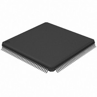
IC MCU AVR32 128KB FLASH 144LQFP
Manufacturer
Atmel
Series
AVR®32 UC3r
Specifications of AT32UC3A0128-ALUT
Core Processor
AVR
Core Size
32-Bit
Speed
66MHz
Connectivity
EBI/EMI, Ethernet, I²C, SPI, SSC, UART/USART, USB OTG
Peripherals
Brown-out Detect/Reset, POR, PWM, WDT
Number Of I /o
109
Program Memory Size
128KB (128K x 8)
Program Memory Type
FLASH
Ram Size
32K x 8
Voltage - Supply (vcc/vdd)
1.65 V ~ 1.95 V
Data Converters
A/D 8x10b
Oscillator Type
Internal
Operating Temperature
-40°C ~ 85°C
Package / Case
144-LQFP
Processor Series
AT32UC3x
Core
AVR32
Data Bus Width
32 bit
Data Ram Size
32 KB
Interface Type
2-Wire, RS-485, SPI, USART
Maximum Clock Frequency
66 MHz
Number Of Programmable I/os
69
Number Of Timers
3
Maximum Operating Temperature
+ 85 C
Mounting Style
SMD/SMT
3rd Party Development Tools
EWAVR32, EWAVR32-BL, KSK-EVK1100-PL
Development Tools By Supplier
ATAVRDRAGON, ATSTK500, ATSTK600, ATAVRISP2, ATAVRONEKIT, ATEXTWIFI, ATEVK1100, ATEVK1105
Minimum Operating Temperature
- 40 C
Controller Family/series
AT32UC3A
No. Of I/o's
109
Ram Memory Size
32KB
Cpu Speed
66MHz
No. Of Timers
1
Rohs Compliant
Yes
For Use With
ATEVK1105 - KIT EVAL FOR AT32UC3A0ATAVRONEKIT - KIT AVR/AVR32 DEBUGGER/PROGRMMR770-1008 - ISP 4PORT ATMEL AVR32 MCU SPIATEVK1100 - KIT DEV/EVAL FOR AVR32 AT32UC3A
Lead Free Status / RoHS Status
Lead free / RoHS Compliant
Eeprom Size
-
Lead Free Status / Rohs Status
Lead free / RoHS Compliant
Available stocks
Company
Part Number
Manufacturer
Quantity
Price
Company:

Part Number:
AT32UC3A0128-ALUT
Manufacturer:
Atmel
Quantity:
166


22.4.2
22.4.3
22.4.4
22.4.5
22.4.6
32058J–AVR32–04/11
I/O Line or Peripheral Function Selection
Peripheral Selection
Output Control
Open Drain Mode
Inputs
When a pin is multiplexed with one or more peripheral functions, the selection is controlled with
the register GPER. If a bit in the register is set, the corresponding pin is controlled by the GPIO.
If a bit is cleared, the corresponding pin is controlled by a peripheral function.
The GPIO provides multiplexing of up to four peripheral functions on a single pin. The selection
is performed by accessing PMR0 (Peripheral Mux Register 0) and PMR1 (Peripheral Mux Regis-
ter 1).
When the I/O line is assigned to a peripheral function, i.e. the corresponding bit in GPER is at 0,
the drive of the I/O line is controlled by the peripheral. The peripheral, depending on the value in
PMR0 and PMR1, determines whether the pin is driven or not.
When the I/O line is controlled by the GPIO, the value of ODER (Output Driver Enable Register)
determines if the pin is driven or not. When a bit in this register is at 1, the corresponding I/O line
is driven by the GPIO. When the bit is at 0, the GPIO does not drive the line.
The level driven on an I/O line can be determined by writing OVR (Output Value Register).
Each I/O line can be independently programmed to operate in open drain mode. This feature
permits several drivers to be connected on the I/O line. The drivers should only actively drive the
line low. An external pull-up resistor (or enabling the internal one) is generally required to guar-
antee a high level on the line when no driver is active.
The Open Drain feature is controlled by ODMER (Open Drain Mode Enable Register). The Open
Drain mode can be selected whether the I/O line is controlled by the GPIO or assigned to a
peripheral function.
The level on each I/O line can be read through PVR (Pin Value Register). This register indicates
the level of the I/O lines regardless of whether the lines are driven by the GPIO or by an external
component. Note that due to power saving measures, PVR register can only be read when
GPER is set for the corresponding pin or if interrupt is enabled for the pin.
Output Line Timings
The figure below shows the timing of the I/O line when setting and clearing the Output Value
Register by accessing OVR. The same timing applies when performing a ‘set’ or ‘clear’ access
i.e. writing to OVRS or OVRC. The timing of PVR (Pin Value Register) is also shown.
AT32UC3A
172
Related parts for AT32UC3A0128-ALUT
Image
Part Number
Description
Manufacturer
Datasheet
Request
R

Part Number:
Description:
DEV KIT FOR AVR/AVR32
Manufacturer:
Atmel
Datasheet:

Part Number:
Description:
INTERVAL AND WIPE/WASH WIPER CONTROL IC WITH DELAY
Manufacturer:
ATMEL Corporation
Datasheet:
Part Number:
Description:
Low-Voltage Voice-Switched IC for Hands-Free Operation
Manufacturer:
ATMEL Corporation
Datasheet:
Part Number:
Description:
MONOLITHIC INTEGRATED FEATUREPHONE CIRCUIT
Manufacturer:
ATMEL Corporation
Datasheet:
Part Number:
Description:
AM-FM Receiver IC U4255BM-M
Manufacturer:
ATMEL Corporation
Datasheet:
Part Number:
Description:
Monolithic Integrated Feature Phone Circuit
Manufacturer:
ATMEL Corporation
Datasheet:
Part Number:
Description:
Multistandard Video-IF and Quasi Parallel Sound Processing
Manufacturer:
ATMEL Corporation
Datasheet:
Part Number:
Description:
High-performance EE PLD
Manufacturer:
ATMEL Corporation
Datasheet:
Part Number:
Description:
8-bit Flash Microcontroller
Manufacturer:
ATMEL Corporation
Datasheet:
Part Number:
Description:
2-Wire Serial EEPROM
Manufacturer:
ATMEL Corporation
Datasheet: