AT32UC3A0128-ALUT Atmel, AT32UC3A0128-ALUT Datasheet - Page 59
AT32UC3A0128-ALUT
Manufacturer Part Number
AT32UC3A0128-ALUT
Description
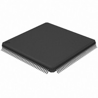
IC MCU AVR32 128KB FLASH 144LQFP
Manufacturer
Atmel
Series
AVR®32 UC3r
Specifications of AT32UC3A0128-ALUT
Core Processor
AVR
Core Size
32-Bit
Speed
66MHz
Connectivity
EBI/EMI, Ethernet, I²C, SPI, SSC, UART/USART, USB OTG
Peripherals
Brown-out Detect/Reset, POR, PWM, WDT
Number Of I /o
109
Program Memory Size
128KB (128K x 8)
Program Memory Type
FLASH
Ram Size
32K x 8
Voltage - Supply (vcc/vdd)
1.65 V ~ 1.95 V
Data Converters
A/D 8x10b
Oscillator Type
Internal
Operating Temperature
-40°C ~ 85°C
Package / Case
144-LQFP
Processor Series
AT32UC3x
Core
AVR32
Data Bus Width
32 bit
Data Ram Size
32 KB
Interface Type
2-Wire, RS-485, SPI, USART
Maximum Clock Frequency
66 MHz
Number Of Programmable I/os
69
Number Of Timers
3
Maximum Operating Temperature
+ 85 C
Mounting Style
SMD/SMT
3rd Party Development Tools
EWAVR32, EWAVR32-BL, KSK-EVK1100-PL
Development Tools By Supplier
ATAVRDRAGON, ATSTK500, ATSTK600, ATAVRISP2, ATAVRONEKIT, ATEXTWIFI, ATEVK1100, ATEVK1105
Minimum Operating Temperature
- 40 C
Controller Family/series
AT32UC3A
No. Of I/o's
109
Ram Memory Size
32KB
Cpu Speed
66MHz
No. Of Timers
1
Rohs Compliant
Yes
For Use With
ATEVK1105 - KIT EVAL FOR AT32UC3A0ATAVRONEKIT - KIT AVR/AVR32 DEBUGGER/PROGRMMR770-1008 - ISP 4PORT ATMEL AVR32 MCU SPIATEVK1100 - KIT DEV/EVAL FOR AVR32 AT32UC3A
Lead Free Status / RoHS Status
Lead free / RoHS Compliant
Eeprom Size
-
Lead Free Status / Rohs Status
Lead free / RoHS Compliant
Available stocks
Company
Part Number
Manufacturer
Quantity
Price
Company:

Part Number:
AT32UC3A0128-ALUT
Manufacturer:
Atmel
Quantity:
166


13.5.5.3
13.5.6
13.5.6.1
13.5.6.2
32058J–AVR32–04/11
Peripheral clock masking
Clock Ready flag
Cautionary note
Mask Ready flag
caler division for the CPU clock by writing CKSEL:CPUDIV to 1 and CPUSEL to the prescaling
value, resulting in a CPU clock frequency:
Similarly, the clock for the PBA, and PBB can be divided by writing their respective bitfields. To
ensure correct operation, frequencies must be selected so that f
must never exceed the specified maximum frequency for each clock domain.
CKSEL can be written without halting or disabling peripheral modules. Writing CKSEL allows a
new clock setting to be written to all synchronous clocks at the same time. It is possible to keep
one or more clocks unchanged by writing the same value a before to the xxxDIV and xxxSEL bit-
fields. This way, it is possible to e.g. scale CPU and HSB speed according to the required
performance, while keeping the PBA and PBB frequency constant.
There is a slight delay from CKSEL is written and the new clock setting becomes effective. Dur-
ing this interval, the Clock Ready (CKRDY) flag in ISR will read as 0. If IER:CKRDY is written to
1, the Power Manager interrupt can be triggered when the new clock setting is effective. CKSEL
must not be re-written while CKRDY is 0, or the system may become unstable or hang.
By default, the clock for all modules are enabled, regardless of which modules are actually being
used. It is possible to disable the clock for a module in the CPU, HSB, PBA, or PBB clock
domain by writing the corresponding bit in the Clock Mask register (CPU/HSB/PBA/PBB) to 0.
When a module is not clocked, it will cease operation, and its registers cannot be read or written.
The module can be re-enabled later by writing the corresponding mask bit to 1.
A module may be connected to several clock domains, in which case it will have several mask
bits.
Table 13-5
Note that clocks should only be switched off if it is certain that the module will not be used.
Switching off the clock for the internal RAM will cause a problem if the stack is mapped there.
Switching off the clock to the Power Manager (PM), which contains the mask registers, or the
corresponding PBx bridge, will make it impossible to write the mask registers again. In this case,
they can only be re-enabled by a system reset.
Due to synchronization in the clock generator, there is a slight delay from a mask register is writ-
ten until the new mask setting goes into effect. When clearing mask bits, this delay can usually
be ignored. However, when setting mask bits, the registers in the corresponding module must
not be written until the clock has actually be re-enabled. The status flag MSKRDY in ISR pro-
vides the required mask status information. When writing either mask register with any value,
this bit is cleared. The bit is set when the clocks have been enabled and disabled according to
the new mask setting. Optionally, the Power Manager interrupt can be enabled by writing the
MSKRDY bit in IER.
f
CPU
= f
contains a list of implemented maskable clocks.
main
/ 2
(CPUSEL+1)
CPU
f
PBA,B
AT32UC3A
. Also, frequencies
59
Related parts for AT32UC3A0128-ALUT
Image
Part Number
Description
Manufacturer
Datasheet
Request
R

Part Number:
Description:
DEV KIT FOR AVR/AVR32
Manufacturer:
Atmel
Datasheet:

Part Number:
Description:
INTERVAL AND WIPE/WASH WIPER CONTROL IC WITH DELAY
Manufacturer:
ATMEL Corporation
Datasheet:
Part Number:
Description:
Low-Voltage Voice-Switched IC for Hands-Free Operation
Manufacturer:
ATMEL Corporation
Datasheet:
Part Number:
Description:
MONOLITHIC INTEGRATED FEATUREPHONE CIRCUIT
Manufacturer:
ATMEL Corporation
Datasheet:
Part Number:
Description:
AM-FM Receiver IC U4255BM-M
Manufacturer:
ATMEL Corporation
Datasheet:
Part Number:
Description:
Monolithic Integrated Feature Phone Circuit
Manufacturer:
ATMEL Corporation
Datasheet:
Part Number:
Description:
Multistandard Video-IF and Quasi Parallel Sound Processing
Manufacturer:
ATMEL Corporation
Datasheet:
Part Number:
Description:
High-performance EE PLD
Manufacturer:
ATMEL Corporation
Datasheet:
Part Number:
Description:
8-bit Flash Microcontroller
Manufacturer:
ATMEL Corporation
Datasheet:
Part Number:
Description:
2-Wire Serial EEPROM
Manufacturer:
ATMEL Corporation
Datasheet: