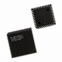
P87C54SBAA,512 NXP Semiconductors, P87C54SBAA,512 Datasheet - Page 40

P87C54SBAA,512
Manufacturer Part Number
P87C54SBAA,512
Description
IC 80C51 MCU 16K OTP 44-PLCC
Manufacturer
NXP Semiconductors
Series
87Cr
Datasheet
1.P87C54SBAA512.pdf
(56 pages)
Specifications of P87C54SBAA,512
Core Processor
8051
Core Size
8-Bit
Speed
16MHz
Connectivity
EBI/EMI, UART/USART
Peripherals
POR
Number Of I /o
32
Program Memory Size
16KB (16K x 8)
Program Memory Type
OTP
Ram Size
256 x 8
Voltage - Supply (vcc/vdd)
2.7 V ~ 5.5 V
Oscillator Type
Internal
Operating Temperature
0°C ~ 70°C
Package / Case
44-PLCC
Processor Series
P87C5x
Core
80C51
Data Bus Width
8 bit
Data Ram Size
256 B
Interface Type
UART
Maximum Clock Frequency
16 MHz
Number Of Programmable I/os
32
Number Of Timers
3
Operating Supply Voltage
2.7 V to 5.5 V
Maximum Operating Temperature
+ 70 C
Mounting Style
SMD/SMT
3rd Party Development Tools
PK51, CA51, A51, ULINK2
Minimum Operating Temperature
0 C
Lead Free Status / RoHS Status
Lead free / RoHS Compliant
Eeprom Size
-
Data Converters
-
Lead Free Status / Rohs Status
Details
Other names
568-1252-5
935258650512
P87C54SBAA
935258650512
P87C54SBAA
Available stocks
Company
Part Number
Manufacturer
Quantity
Price
Company:
Part Number:
P87C54SBAA,512
Manufacturer:
NXP Semiconductors
Quantity:
10 000
Philips Semiconductors
EXPLANATION OF THE AC SYMBOLS
Each timing symbol has five characters. The first character is always
‘t’ (= time). The other characters, depending on their positions,
indicate the name of a signal or the logical status of that signal. The
designations are:
A – Address
C – Clock
D – Input data
H – Logic level high
I – Instruction (program memory contents)
L – Logic level low, or ALE
2000 Aug 07
PORT 0
PORT 2
80C51 8-bit microcontroller family
8K–64K/256–1K OTP/ROM/ROMless, low voltage (2.7V–5.5V),
low power, high speed (33MHz)
PSEN
ALE
RD
PORT 0
PORT 2
PSEN
ALE
t
AVLL
FROM RI OR DPL
A0–A7
t
LLAX
t
t
AVWL
LHLL
t
t
LLWL
AVLL
A0–A7
Figure 29. External Program Memory Read Cycle
t
t
AVDV
P2.0–P2.7 OR A8–A15 FROM DPF
RLAZ
Figure 30. External Data Memory Read Cycle
t
LLDV
t
t
t
AVIV
LLAX
LLPL
t
LLIV
t
t
PLIV
RLDV
A0–A15
t
PLAZ
t
PLPH
t
RLRH
t
PXIX
INSTR IN
40
t
RHDX
DATA IN
P – PSEN
Q – Output data
R – RD signal
t – Time
V – Valid
W – WR signal
X – No longer a valid logic level
Z – Float
Examples: t
t
PXIZ
t
RHDZ
t
t
AVLL
WHLH
LLPL
8XC51RA+/RB+/RC+/RD+/80C51RA+
= Time for address valid to ALE low.
=Time for ALE low to PSEN low.
A0–A7
A0–A7 FROM PCL
A0–A15 FROM PCH
8XC51FA/FB/FC/80C51FA
A8–A15
Product specification
SU00006
8XC54/58
INSTR IN
SU00025


