LPC1754FBD80,551 NXP Semiconductors, LPC1754FBD80,551 Datasheet - Page 30
LPC1754FBD80,551
Manufacturer Part Number
LPC1754FBD80,551
Description
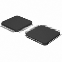
IC ARM CORTEX MCU 128K 80-LQFP
Manufacturer
NXP Semiconductors
Series
LPC17xxr
Specifications of LPC1754FBD80,551
Program Memory Type
FLASH
Program Memory Size
128KB (128K x 8)
Package / Case
80-LQFP
Core Processor
ARM® Cortex-M3™
Core Size
32-Bit
Speed
100MHz
Connectivity
CAN, I²C, IrDA, Microwire, SPI, SSI, SSP, UART/USART, USB OTG
Peripherals
Brown-out Detect/Reset, DMA, Motor Control PWM, POR, PWM, WDT
Number Of I /o
52
Ram Size
32K x 8
Voltage - Supply (vcc/vdd)
2.4 V ~ 3.6 V
Data Converters
A/D 6x12b, D/A 1x10b
Oscillator Type
Internal
Operating Temperature
-40°C ~ 85°C
Processor Series
LPC17
Core
ARM Cortex M3
Data Bus Width
32 bit
Data Ram Size
32 KB
Interface Type
CAN, I2C, SPI, UART
Maximum Clock Frequency
100 MHz
Number Of Programmable I/os
52
Number Of Timers
3
Operating Supply Voltage
3.3 V
Maximum Operating Temperature
+ 85 C
Mounting Style
SMD/SMT
3rd Party Development Tools
MDK-ARM, RL-ARM, ULINK2
Minimum Operating Temperature
- 40 C
On-chip Adc
12 bit, 6 Channel
On-chip Dac
10 bit
Cpu Family
LPC17xx
Device Core
ARM Cortex-M3
Device Core Size
32b
Frequency (max)
100MHz
Total Internal Ram Size
32KB
# I/os (max)
52
Number Of Timers - General Purpose
4
Operating Supply Voltage (typ)
3.3V
Operating Supply Voltage (max)
3.6V
Operating Supply Voltage (min)
2.4/2.7V
Instruction Set Architecture
RISC
Operating Temp Range
-40C to 85C
Operating Temperature Classification
Industrial
Mounting
Surface Mount
Pin Count
80
Package Type
LQFP
Lead Free Status / RoHS Status
Lead free / RoHS Compliant
For Use With
622-1005 - USB IN-CIRCUIT PROG ARM7 LPC2K
Eeprom Size
-
Lead Free Status / Rohs Status
Lead free / RoHS Compliant
Other names
568-4790
935287913551
935287913551
Available stocks
Company
Part Number
Manufacturer
Quantity
Price

Company:
Part Number:
LPC1754FBD80,551
Manufacturer:
NXP Semiconductors
Quantity:
10 000
Part Number:
LPC1754FBD80,551
Manufacturer:
NXP/恩智浦
Quantity:
20 000


NXP Semiconductors
LPC1759_58_56_54_52_51
Product data sheet
7.29.2 Main PLL (PLL0)
7.29.3 USB PLL (PLL1)
7.29.4 Wake-up timer
The PLL0 accepts an input clock frequency in the range of 32 kHz to 25 MHz. The input
frequency is multiplied up to a high frequency, then divided down to provide the actual
clock used by the CPU and/or the USB block.
The PLL0 input, in the range of 32 kHz to 25 MHz, may initially be divided down by a
value ‘N’, which may be in the range of 1 to 256. This input division provides a wide range
of output frequencies from the same input frequency.
Following the PLL0 input divider is the PLL0 multiplier. This can multiply the input divider
output through the use of a Current Controlled Oscillator (CCO) by a value ‘M’, in the
range of 1 through 32768. The resulting frequency must be in the range of 275 MHz to
550 MHz. The multiplier works by dividing the CCO output by the value of M, then using a
phase-frequency detector to compare the divided CCO output to the multiplier input. The
error value is used to adjust the CCO frequency.
The PLL0 is turned off and bypassed following a chip Reset and by entering Power-down
mode. PLL0 is enabled by software only. The program must configure and activate the
PLL0, wait for the PLL0 to lock, and then connect to the PLL0 as a clock source.
The LPC1759/58/56/54/52/51 contain a second, dedicated USB PLL1 to provide clocking
for the USB interface.
The PLL1 receives its clock input from the main oscillator only and provides a fixed
48 MHz clock to the USB block only. The PLL1 is disabled and powered off on reset. If the
PLL1 is left disabled, the USB clock will be supplied by the 48 MHz clock from the main
PLL0.
The PLL1 accepts an input clock frequency in the range of 10 MHz to 25 MHz only. The
input frequency is multiplied up the range of 48 MHz for the USB clock using a Current
Controlled Oscillators (CCO). It is insured that the PLL1 output has a 50 % duty cycle.
The LPC1759/58/56/54/52/51 begin operation at power-up and when awakened from
Power-down mode by using the 4 MHz IRC oscillator as the clock source. This allows chip
operation to resume quickly. If the main oscillator or the PLL is needed by the application,
software will need to enable these features and wait for them to stabilize before they are
used as a clock source.
When the main oscillator is initially activated, the wake-up timer allows software to ensure
that the main oscillator is fully functional before the processor uses it as a clock source
and starts to execute instructions. This is important at power on, all types of Reset, and
whenever any of the aforementioned functions are turned off for any reason. Since the
oscillator and other functions are turned off during Power-down mode, any wake-up of the
processor from Power-down mode makes use of the wake-up Timer.
The Wake-up Timer monitors the crystal oscillator to check whether it is safe to begin
code execution. When power is applied to the chip, or when some event caused the chip
to exit Power-down mode, some time is required for the oscillator to produce a signal of
sufficient amplitude to drive the clock logic. The amount of time depends on many factors,
including the rate of V
All information provided in this document is subject to legal disclaimers.
DD(3V3)
Rev. 6.01 — 11 March 2011
ramp (in the case of power on), the type of crystal and its
LPC1759/58/56/54/52/51
32-bit ARM Cortex-M3 microcontroller
© NXP B.V. 2011. All rights reserved.
30 of 74
Related parts for LPC1754FBD80,551
Image
Part Number
Description
Manufacturer
Datasheet
Request
R

Part Number:
Description:
32-bit ARM Cortex-M3 MCU; up to 512 kB flash and 64 kB SRAM with Ethernet, USB 2.0 Host/Device/OTG, CAN
Manufacturer:
NXP [NXP Semiconductors]
Datasheet:

Part Number:
Description:
NXP Semiconductors designed the LPC2420/2460 microcontroller around a 16-bit/32-bitARM7TDMI-S CPU core with real-time debug interfaces that include both JTAG andembedded trace
Manufacturer:
NXP Semiconductors
Datasheet:

Part Number:
Description:
NXP Semiconductors designed the LPC2458 microcontroller around a 16-bit/32-bitARM7TDMI-S CPU core with real-time debug interfaces that include both JTAG andembedded trace
Manufacturer:
NXP Semiconductors
Datasheet:
Part Number:
Description:
NXP Semiconductors designed the LPC2468 microcontroller around a 16-bit/32-bitARM7TDMI-S CPU core with real-time debug interfaces that include both JTAG andembedded trace
Manufacturer:
NXP Semiconductors
Datasheet:
Part Number:
Description:
NXP Semiconductors designed the LPC2470 microcontroller, powered by theARM7TDMI-S core, to be a highly integrated microcontroller for a wide range ofapplications that require advanced communications and high quality graphic displays
Manufacturer:
NXP Semiconductors
Datasheet:
Part Number:
Description:
NXP Semiconductors designed the LPC2478 microcontroller, powered by theARM7TDMI-S core, to be a highly integrated microcontroller for a wide range ofapplications that require advanced communications and high quality graphic displays
Manufacturer:
NXP Semiconductors
Datasheet:
Part Number:
Description:
The Philips Semiconductors XA (eXtended Architecture) family of 16-bit single-chip microcontrollers is powerful enough to easily handle the requirements of high performance embedded applications, yet inexpensive enough to compete in the market for hi
Manufacturer:
NXP Semiconductors
Datasheet:
Part Number:
Description:
The XA-S3 device is a member of Philips Semiconductors? XA(eXtended Architecture) family of high performance 16-bitsingle-chip microcontrollers
Manufacturer:
NXP Semiconductors
Datasheet:

Part Number:
Description:
The NXP BlueStreak LH75401/LH75411 family consists of two low-cost 16/32-bit System-on-Chip (SoC) devices
Manufacturer:
NXP Semiconductors
Datasheet:
Part Number:
Description:
The NXP LPC3130/3131 combine an 180 MHz ARM926EJ-S CPU core, high-speed USB2
Manufacturer:
NXP Semiconductors
Datasheet:
Part Number:
Description:
The NXP LPC3141 combine a 270 MHz ARM926EJ-S CPU core, High-speed USB 2
Manufacturer:
NXP Semiconductors
Part Number:
Description:
The NXP LPC3143 combine a 270 MHz ARM926EJ-S CPU core, High-speed USB 2
Manufacturer:
NXP Semiconductors

Part Number:
Description:
The NXP LPC3152 combines an 180 MHz ARM926EJ-S CPU core, High-speed USB 2
Manufacturer:
NXP Semiconductors
Part Number:
Description:
The NXP LPC3154 combines an 180 MHz ARM926EJ-S CPU core, High-speed USB 2
Manufacturer:
NXP Semiconductors