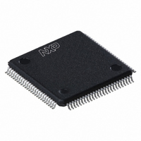
LPC1764FBD100,551 NXP Semiconductors, LPC1764FBD100,551 Datasheet - Page 30

LPC1764FBD100,551
Manufacturer Part Number
LPC1764FBD100,551
Description
IC ARM CORTEX MCU 128K 100-LQFP
Manufacturer
NXP Semiconductors
Series
LPC17xxr
Specifications of LPC1764FBD100,551
Program Memory Type
FLASH
Program Memory Size
128KB (128K x 8)
Package / Case
100-LQFP
Core Processor
ARM® Cortex-M3™
Core Size
32-Bit
Speed
100MHz
Connectivity
CAN, Ethernet, I²C, IrDA, Microwire, SPI, SSI, UART/USART, USB
Peripherals
Brown-out Detect/Reset, DMA, Motor Control PWM, POR, PWM, WDT
Number Of I /o
70
Ram Size
32K x 8
Voltage - Supply (vcc/vdd)
2.4 V ~ 3.6 V
Data Converters
A/D 8x12b
Oscillator Type
Internal
Operating Temperature
-40°C ~ 85°C
Processor Series
LPC17
Core
ARM Cortex M3
Data Bus Width
32 bit
Data Ram Size
32 KB
Interface Type
CAN, I2C, SPI, UART
Maximum Clock Frequency
100 MHz
Number Of Programmable I/os
70
Number Of Timers
3
Operating Supply Voltage
3.3 V
Maximum Operating Temperature
+ 85 C
Mounting Style
SMD/SMT
3rd Party Development Tools
MDK-ARM, RL-ARM, ULINK2, MCB1760, MCB1760U, MCB1760UME, IRD-LPC1768-DEV, KSK-LPC1768-JL
Minimum Operating Temperature
- 40 C
On-chip Adc
12 bit, 8 Channel
On-chip Dac
10 bit
Package
100LQFP
Device Core
ARM Cortex M3
Family Name
LPC1700
Maximum Speed
100 MHz
Lead Free Status / RoHS Status
Lead free / RoHS Compliant
For Use With
622-1005 - USB IN-CIRCUIT PROG ARM7 LPC2K
Eeprom Size
-
Lead Free Status / Rohs Status
Lead free / RoHS Compliant
Other names
568-4793
935287919551
935287919551
Available stocks
Company
Part Number
Manufacturer
Quantity
Price
Company:
Part Number:
LPC1764FBD100,551
Manufacturer:
NXP Semiconductors
Quantity:
10 000
NXP Semiconductors
LPC1769_68_67_66_65_64_63
Product data sheet
7.22.1 Features
7.22 Pulse width modulator
The PWM is based on the standard Timer block and inherits all of its features, although
only the PWM function is pinned out on the LPC17xx. The Timer is designed to count
cycles of the system derived clock and optionally switch pins, generate interrupts or
perform other actions when specified timer values occur, based on seven match registers.
The PWM function is in addition to these features, and is based on match register events.
The ability to separately control rising and falling edge locations allows the PWM to be
used for more applications. For instance, multi-phase motor control typically requires
three non-overlapping PWM outputs with individual control of all three pulse widths and
positions.
Two match registers can be used to provide a single edge controlled PWM output. One
match register (PWMMR0) controls the PWM cycle rate, by resetting the count upon
match. The other match register controls the PWM edge position. Additional single edge
controlled PWM outputs require only one match register each, since the repetition rate is
the same for all PWM outputs. Multiple single edge controlled PWM outputs will all have a
rising edge at the beginning of each PWM cycle, when an PWMMR0 match occurs.
Three match registers can be used to provide a PWM output with both edges controlled.
Again, the PWMMR0 match register controls the PWM cycle rate. The other match
registers control the two PWM edge positions. Additional double edge controlled PWM
outputs require only two match registers each, since the repetition rate is the same for all
PWM outputs.
With double edge controlled PWM outputs, specific match registers control the rising and
falling edge of the output. This allows both positive going PWM pulses (when the rising
edge occurs prior to the falling edge), and negative going PWM pulses (when the falling
edge occurs prior to the rising edge).
•
•
•
•
Up to four external outputs corresponding to match registers, with the following
capabilities:
– Set LOW on match.
– Set HIGH on match.
– Toggle on match.
– Do nothing on match.
Up to two match registers can be used to generate timed DMA requests.
One PWM block with Counter or Timer operation (may use the peripheral clock or one
of the capture inputs as the clock source).
Seven match registers allow up to 6 single edge controlled or 3 double edge
controlled PWM outputs, or a mix of both types. The match registers also allow:
– Continuous operation with optional interrupt generation on match.
– Stop timer on match with optional interrupt generation.
– Reset timer on match with optional interrupt generation.
All information provided in this document is subject to legal disclaimers.
Rev. 6.01 — 11 March 2011
LPC1769/68/67/66/65/64/63
32-bit ARM Cortex-M3 microcontroller
© NXP B.V. 2011. All rights reserved.
30 of 79


