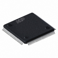
LPC1764FBD100,551 NXP Semiconductors, LPC1764FBD100,551 Datasheet - Page 39

LPC1764FBD100,551
Manufacturer Part Number
LPC1764FBD100,551
Description
IC ARM CORTEX MCU 128K 100-LQFP
Manufacturer
NXP Semiconductors
Series
LPC17xxr
Specifications of LPC1764FBD100,551
Program Memory Type
FLASH
Program Memory Size
128KB (128K x 8)
Package / Case
100-LQFP
Core Processor
ARM® Cortex-M3™
Core Size
32-Bit
Speed
100MHz
Connectivity
CAN, Ethernet, I²C, IrDA, Microwire, SPI, SSI, UART/USART, USB
Peripherals
Brown-out Detect/Reset, DMA, Motor Control PWM, POR, PWM, WDT
Number Of I /o
70
Ram Size
32K x 8
Voltage - Supply (vcc/vdd)
2.4 V ~ 3.6 V
Data Converters
A/D 8x12b
Oscillator Type
Internal
Operating Temperature
-40°C ~ 85°C
Processor Series
LPC17
Core
ARM Cortex M3
Data Bus Width
32 bit
Data Ram Size
32 KB
Interface Type
CAN, I2C, SPI, UART
Maximum Clock Frequency
100 MHz
Number Of Programmable I/os
70
Number Of Timers
3
Operating Supply Voltage
3.3 V
Maximum Operating Temperature
+ 85 C
Mounting Style
SMD/SMT
3rd Party Development Tools
MDK-ARM, RL-ARM, ULINK2, MCB1760, MCB1760U, MCB1760UME, IRD-LPC1768-DEV, KSK-LPC1768-JL
Minimum Operating Temperature
- 40 C
On-chip Adc
12 bit, 8 Channel
On-chip Dac
10 bit
Package
100LQFP
Device Core
ARM Cortex M3
Family Name
LPC1700
Maximum Speed
100 MHz
Lead Free Status / RoHS Status
Lead free / RoHS Compliant
For Use With
622-1005 - USB IN-CIRCUIT PROG ARM7 LPC2K
Eeprom Size
-
Lead Free Status / Rohs Status
Lead free / RoHS Compliant
Other names
568-4793
935287919551
935287919551
Available stocks
Company
Part Number
Manufacturer
Quantity
Price
Company:
Part Number:
LPC1764FBD100,551
Manufacturer:
NXP Semiconductors
Quantity:
10 000
NXP Semiconductors
LPC1769_68_67_66_65_64_63
Product data sheet
7.30.1 Reset
7.30 System control
Reset has four sources on the LPC17xx: the RESET pin, the Watchdog reset, power-on
reset (POR), and the BrownOut Detection (BOD) circuit. The RESET pin is a Schmitt
trigger input pin. Assertion of chip Reset by any source, once the operating voltage attains
a usable level, causes the RSTOUT pin to go LOW and starts the wake-up timer (see
description in
until the external Reset is de-asserted, the oscillator is running, a fixed number of clocks
have passed, and the flash controller has completed its initialization. Once reset is
de-asserted, or, in case of a BOD-triggered reset, once the voltage rises above the BOD
threshold, the RSTOUT pin goes HIGH.
When the internal Reset is removed, the processor begins executing at address 0, which
is initially the Reset vector mapped from the Boot Block. At that point, all of the processor
and peripheral registers have been initialized to predetermined values.
Fig 6.
Power distribution
V
DD(REG)(3V3)
Section
All information provided in this document is subject to legal disclaimers.
V
VREFN
DD(3V3)
RTCX1
RTCX2
VREFP
VBAT
V
V
V
DDA
SSA
SS
7.29.5). The wake-up timer ensures that reset remains asserted
Rev. 6.01 — 11 March 2011
LPC17xx
LPC1769/68/67/66/65/64/63
RTC POWER DOMAIN
ADC POWER DOMAIN
MAIN POWER DOMAIN
OSCILLATOR
SELECTOR
to I/O pads
POWER
32 kHz
REGULATOR
32-bit ARM Cortex-M3 microcontroller
ULTRA LOW-POWER
REGULATOR
DAC
ADC
BACKUP REGISTERS
REAL-TIME CLOCK
to core
to memories,
peripherals,
oscillators,
PLLs
002aad978
© NXP B.V. 2011. All rights reserved.
39 of 79


