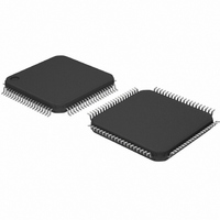
LPC1758FBD80,551 NXP Semiconductors, LPC1758FBD80,551 Datasheet - Page 35

LPC1758FBD80,551
Manufacturer Part Number
LPC1758FBD80,551
Description
IC ARM CORTEX MCU 512K 80-LQFP
Manufacturer
NXP Semiconductors
Series
LPC17xxr
Specifications of LPC1758FBD80,551
Program Memory Type
FLASH
Program Memory Size
512KB (512K x 8)
Package / Case
80-LQFP
Core Processor
ARM® Cortex-M3™
Core Size
32-Bit
Speed
100MHz
Connectivity
CAN, Ethernet, I²C, IrDA, Microwire, SPI, SSI, UART/USART, USB OTG
Peripherals
Brown-out Detect/Reset, DMA, I²S, Motor Control PWM, POR, PWM, WDT
Number Of I /o
52
Ram Size
64K x 8
Voltage - Supply (vcc/vdd)
2.4 V ~ 3.6 V
Data Converters
A/D 6x12b, D/A 1x10b
Oscillator Type
Internal
Operating Temperature
-40°C ~ 85°C
Processor Series
LPC17
Core
ARM Cortex M3
Data Bus Width
32 bit
Data Ram Size
64 KB
Interface Type
CAN, I2C, SPI, UART
Maximum Clock Frequency
100 MHz
Number Of Programmable I/os
52
Number Of Timers
3
Operating Supply Voltage
3.3 V
Maximum Operating Temperature
+ 85 C
Mounting Style
SMD/SMT
3rd Party Development Tools
MDK-ARM, RL-ARM, ULINK2
Development Tools By Supplier
OM11036
Minimum Operating Temperature
- 40 C
On-chip Adc
12 bit, 6 Channel
On-chip Dac
10 bit
Package
80LQFP
Device Core
ARM Cortex M3
Family Name
LPC17xx
Maximum Speed
100 MHz
Cpu Family
LPC17xx
Device Core Size
32b
Frequency (max)
100MHz
Total Internal Ram Size
64KB
# I/os (max)
52
Number Of Timers - General Purpose
4
Operating Supply Voltage (typ)
3.3V
Operating Supply Voltage (max)
3.6V
Operating Supply Voltage (min)
2.4/2.7V
Instruction Set Architecture
RISC
Operating Temp Range
-40C to 85C
Operating Temperature Classification
Industrial
Mounting
Surface Mount
Pin Count
80
Package Type
LQFP
Lead Free Status / RoHS Status
Lead free / RoHS Compliant
For Use With
622-1005 - USB IN-CIRCUIT PROG ARM7 LPC2K
Eeprom Size
-
Lead Free Status / Rohs Status
Lead free / RoHS Compliant
Other names
568-4792
935288607551
935288607551
Available stocks
Company
Part Number
Manufacturer
Quantity
Price
Company:
Part Number:
LPC1758FBD80,551
Manufacturer:
NXP Semiconductors
Quantity:
10 000
NXP Semiconductors
1.
LPC1759_58_56_54_52_51
Product data sheet
CAUTION
LPC1751FBD80 with device ID 25001110 does not support CRP feature. LPC1751FBD80 with device ID 25001118 does support
CRP. See errata note in ES_LPC1751.
7.30.2 Brownout detection
7.30.3 Code security (Code Read Protection - CRP)
7.30.4 APB interface
The LPC1759/58/56/54/52/51 include 2-stage monitoring of the voltage on the
V
the Vectored Interrupt Controller. This signal can be enabled for interrupt in the Interrupt
Enable Register in the NVIC in order to cause a CPU interrupt; if not, software can monitor
the signal by reading a dedicated status register.
The second stage of low-voltage detection asserts reset to inactivate the
LPC1759/58/56/54/52/51 when the voltage on the V
This reset prevents alteration of the flash as operation of the various elements of the chip
would otherwise become unreliable due to low voltage. The BOD circuit maintains this
reset down below 1 V, at which point the power-on reset circuitry maintains the overall
reset.
Both the 2.2 V and 1.85 V thresholds include some hysteresis. In normal operation, this
hysteresis allows the 2.2 V detection to reliably interrupt, or a regularly executed event
loop to sense the condition.
This feature of the LPC1759/58/56/54/52/51 allows user to enable different levels of
security in the system so that access to the on-chip flash and use of the JTAG and ISP
can be restricted. When needed, CRP is invoked by programming a specific pattern into a
dedicated flash location. IAP commands are not affected by the CRP.
There are three levels of the Code Read Protection.
CRP1 disables access to chip via the JTAG and allows partial flash update (excluding
flash sector 0) using a limited set of the ISP commands. This mode is useful when CRP is
required and flash field updates are needed but all sectors can not be erased.
CRP2 disables access to chip via the JTAG and only allows full flash erase and update
using a reduced set of the ISP commands.
Running an application with level CRP3 selected fully disables any access to chip via the
JTAG pins and the ISP. This mode effectively disables ISP override using P2[10] pin, too.
It is up to the user’s application to provide (if needed) flash update mechanism using IAP
calls or call reinvoke ISP command to enable flash update via UART0.
The APB peripherals are split into two separate APB buses in order to distribute the bus
bandwidth and thereby reducing stalls caused by contention between the CPU and the
GPDMA controller.
DD(REG)(3V3)
If level three Code Read Protection (CRP3) is selected, no future factory testing can be
performed on the device.
pins. If this voltage falls below 2.2 V, the BOD asserts an interrupt signal to
All information provided in this document is subject to legal disclaimers.
Rev. 6.01 — 11 March 2011
LPC1759/58/56/54/52/51
32-bit ARM Cortex-M3 microcontroller
DD(REG)(3V3)
1
pins falls below 1.85 V.
© NXP B.V. 2011. All rights reserved.
35 of 74


