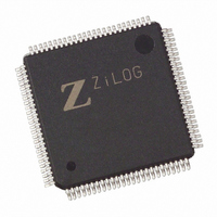
EZ80F92AZ020EG Zilog, EZ80F92AZ020EG Datasheet - Page 135

EZ80F92AZ020EG
Manufacturer Part Number
EZ80F92AZ020EG
Description
IC ACCLAIM MCU 128KB 100LQFP
Manufacturer
Zilog
Series
eZ80® Acclaim!®r
Specifications of EZ80F92AZ020EG
Core Processor
Z8
Core Size
8-Bit
Speed
20MHz
Connectivity
I²C, IrDA, SPI, UART/USART
Peripherals
Brown-out Detect/Reset, POR, WDT
Number Of I /o
24
Program Memory Size
128KB (128K x 8)
Program Memory Type
FLASH
Ram Size
8K x 8
Voltage - Supply (vcc/vdd)
3 V ~ 3.6 V
Oscillator Type
Internal
Operating Temperature
-40°C ~ 105°C
Package / Case
100-LQFP
Processor Series
EZ80F92x
Core
eZ80
Data Bus Width
8 bit
Data Ram Size
8 KB
Interface Type
I2C, IrDA, SPI, UART
Maximum Clock Frequency
20 MHz
Number Of Programmable I/os
24
Number Of Timers
6
Operating Supply Voltage
3 V to 3.6 V
Maximum Operating Temperature
+ 105 C
Mounting Style
SMD/SMT
Development Tools By Supplier
eZ80F920200ZCOG
Minimum Operating Temperature
- 40 C
Lead Free Status / RoHS Status
Lead free / RoHS Compliant
Eeprom Size
-
Data Converters
-
Lead Free Status / Rohs Status
Details
Other names
269-3871
EZ80F92AZ020EG
EZ80F92AZ020EG
Available stocks
Company
Part Number
Manufacturer
Quantity
Price
- Current page: 135 of 261
- Download datasheet (4Mb)
Table 69. GPIO Mode Selection when using the IrDA Encoder/Decoder
PS015313-0508
GPIO Port D Bits
PD0
PD1
PD2–PD7
Jitter
Infrared Encoder/Decoder Signal Pins
Loopback Testing
Setting the upper 4 bits of IR_CTL to
receiver. In this mode, the IrDA receiver uses edge detection on the IR_RxD bit stream.
Due to the inherent sampling of the received IR_RxD signal by the BIt Rate Clock, some
jitter can be expected on the first bit in any sequence of data. However, all subsequent bits
in the received data stream are a fixed 16 clock periods wide.
The IrDA endec signal pins (IR_TxD and IR_RxD) are multiplexed with General-Purpose
I/O (GPIO) pins. These GPIO pins must be configured for alternate function operation for
the endec to operate.
The remaining six UART0 pins (CTS0, DCD0, DSR0, DTR0, RTS and RI0) are not
required for use with the endec. The UART0 modem status interrupt should be disabled to
prevent unwanted interrupts from these pins. The GPIO pins corresponding to these six
unused UART0 pins can be used for inputs, outputs, or interrupt sources. Recommended
GPIO Port D control register settings are provided in
Input/Output on page 39 for additional information about setting the GPIO Port modes.
Both internal and external loopback testing can be accomplished with the IrDA endec on
the eZ80F92 device. Setting the LOOP_BACK bit to 1 enables internal loopback testing.
During internal loopback, the IR_TxD output signal is inverted and connected on-chip to
the IR_RxD input. External loopback testing of the off-chip IrDA transceiver can be
accomplished by transmitting data from the UART while the receiver is enabled
(IR_RxEN set to 1).
Allowable GPIO
Port Mode
7
7
Any other than GPIO Mode 7
(1, 2, 3, 4, 5, 6, 8, or 9)
00h
Alternate function.
Alternate function.
Allowable Port Mode Functions
Output, input, open-drain, open-source, level-
sensitive interrupt input, or edge-triggered
interrupt input.
disables the frequency divider but not the IrDA
Table
69. See General-Purpose
Product Specification
Infrared Encoder/Decoder
128
Related parts for EZ80F92AZ020EG
Image
Part Number
Description
Manufacturer
Datasheet
Request
R

Part Number:
Description:
Communication Controllers, ZILOG INTELLIGENT PERIPHERAL CONTROLLER (ZIP)
Manufacturer:
Zilog, Inc.
Datasheet:

Part Number:
Description:
KIT DEV FOR Z8 ENCORE 16K TO 64K
Manufacturer:
Zilog
Datasheet:

Part Number:
Description:
KIT DEV Z8 ENCORE XP 28-PIN
Manufacturer:
Zilog
Datasheet:

Part Number:
Description:
DEV KIT FOR Z8 ENCORE 8K/4K
Manufacturer:
Zilog
Datasheet:

Part Number:
Description:
KIT DEV Z8 ENCORE XP 28-PIN
Manufacturer:
Zilog
Datasheet:

Part Number:
Description:
DEV KIT FOR Z8 ENCORE 4K TO 8K
Manufacturer:
Zilog
Datasheet:

Part Number:
Description:
CMOS Z8 microcontroller. ROM 16 Kbytes, RAM 256 bytes, speed 16 MHz, 32 lines I/O, 3.0V to 5.5V
Manufacturer:
Zilog, Inc.
Datasheet:

Part Number:
Description:
Low-cost microcontroller. 512 bytes ROM, 61 bytes RAM, 8 MHz
Manufacturer:
Zilog, Inc.
Datasheet:

Part Number:
Description:
Z8 4K OTP Microcontroller
Manufacturer:
Zilog, Inc.
Datasheet:

Part Number:
Description:
CMOS SUPER8 ROMLESS MCU
Manufacturer:
Zilog, Inc.
Datasheet:

Part Number:
Description:
SL1866 CMOSZ8 OTP Microcontroller
Manufacturer:
Zilog, Inc.
Datasheet:

Part Number:
Description:
SL1866 CMOSZ8 OTP Microcontroller
Manufacturer:
Zilog, Inc.
Datasheet:

Part Number:
Description:
OTP (KB) = 1, RAM = 125, Speed = 12, I/O = 14, 8-bit Timers = 2, Comm Interfaces Other Features = Por, LV Protect, Voltage = 4.5-5.5V
Manufacturer:
Zilog, Inc.
Datasheet:

Part Number:
Description:
Manufacturer:
Zilog, Inc.
Datasheet:


