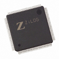
EZ80F92AZ020EG Zilog, EZ80F92AZ020EG Datasheet - Page 206

EZ80F92AZ020EG
Manufacturer Part Number
EZ80F92AZ020EG
Description
IC ACCLAIM MCU 128KB 100LQFP
Manufacturer
Zilog
Series
eZ80® Acclaim!®r
Specifications of EZ80F92AZ020EG
Core Processor
Z8
Core Size
8-Bit
Speed
20MHz
Connectivity
I²C, IrDA, SPI, UART/USART
Peripherals
Brown-out Detect/Reset, POR, WDT
Number Of I /o
24
Program Memory Size
128KB (128K x 8)
Program Memory Type
FLASH
Ram Size
8K x 8
Voltage - Supply (vcc/vdd)
3 V ~ 3.6 V
Oscillator Type
Internal
Operating Temperature
-40°C ~ 105°C
Package / Case
100-LQFP
Processor Series
EZ80F92x
Core
eZ80
Data Bus Width
8 bit
Data Ram Size
8 KB
Interface Type
I2C, IrDA, SPI, UART
Maximum Clock Frequency
20 MHz
Number Of Programmable I/os
24
Number Of Timers
6
Operating Supply Voltage
3 V to 3.6 V
Maximum Operating Temperature
+ 105 C
Mounting Style
SMD/SMT
Development Tools By Supplier
eZ80F920200ZCOG
Minimum Operating Temperature
- 40 C
Lead Free Status / RoHS Status
Lead free / RoHS Compliant
Eeprom Size
-
Data Converters
-
Lead Free Status / Rohs Status
Details
Other names
269-3871
EZ80F92AZ020EG
EZ80F92AZ020EG
Available stocks
Company
Part Number
Manufacturer
Quantity
Price
- Current page: 206 of 261
- Download datasheet (4Mb)
PS015313-0508
Table 114. Flash Data Register; (FLASH_DATA = 00F6h)
Flash Address Upper Byte Register
The FLASH_ADDR_U register defines the upper 7 bits of the address for Flash memory.
Changing the value of FLASH_ADDR_U allows the on-chip 128 KB/64 KB Flash
memory to be mapped to any location within the 16 MB linear address space of the
eZ80F92 device. If the on-chip Flash memory is enabled, Flash address assumes priority
over any external Chip Selects. The external Chip Select signals are not asserted if the
corresponding Flash address is enabled. The internal Flash memory does not hold priority
over internal SRAM.
Table 115. Flash Address Upper Byte Register; (FLASH_ADDR_U = 00F7h)
Bit
Reset
CPU Access
Note: R/W = Read/Write.
Bit
Position
[7:0]
FLASH_DATA
Bit
Reset
CPU Access
Note: R/W = Read/Write; R = Read Only.
Bit
Position
[7:1]
FLASH_ADDR_U
0
Value Description
00h–
FFh
Value Description
00h–
FEh
0
R/W
Data value to be written to Flash during an I/O Write operation.
R/W
X
7
7
0
These bits define the upper byte of the Flash address. When
on-chip Flash is enabled, the Flash address space begins at
address {FLASH_ADDR_U, 0b, 0000h}. On-chip Flash is
prioritized over all external Chip Selects.
Reserved (enforces alignment on a 128 KB boundary).
R/W
R/W
X
6
6
0
R/W
R/W
X
5
5
0
R/W
R/W
X
4
4
0
R/W
R/W
X
3
3
0
Product Specification
R/W
R/W
X
2
2
0
eZ80F92/eZ80F93
R/W
R/W
X
1
1
0
Flash Memory
R/W
X
R
0
0
0
199
Related parts for EZ80F92AZ020EG
Image
Part Number
Description
Manufacturer
Datasheet
Request
R

Part Number:
Description:
Communication Controllers, ZILOG INTELLIGENT PERIPHERAL CONTROLLER (ZIP)
Manufacturer:
Zilog, Inc.
Datasheet:

Part Number:
Description:
KIT DEV FOR Z8 ENCORE 16K TO 64K
Manufacturer:
Zilog
Datasheet:

Part Number:
Description:
KIT DEV Z8 ENCORE XP 28-PIN
Manufacturer:
Zilog
Datasheet:

Part Number:
Description:
DEV KIT FOR Z8 ENCORE 8K/4K
Manufacturer:
Zilog
Datasheet:

Part Number:
Description:
KIT DEV Z8 ENCORE XP 28-PIN
Manufacturer:
Zilog
Datasheet:

Part Number:
Description:
DEV KIT FOR Z8 ENCORE 4K TO 8K
Manufacturer:
Zilog
Datasheet:

Part Number:
Description:
CMOS Z8 microcontroller. ROM 16 Kbytes, RAM 256 bytes, speed 16 MHz, 32 lines I/O, 3.0V to 5.5V
Manufacturer:
Zilog, Inc.
Datasheet:

Part Number:
Description:
Low-cost microcontroller. 512 bytes ROM, 61 bytes RAM, 8 MHz
Manufacturer:
Zilog, Inc.
Datasheet:

Part Number:
Description:
Z8 4K OTP Microcontroller
Manufacturer:
Zilog, Inc.
Datasheet:

Part Number:
Description:
CMOS SUPER8 ROMLESS MCU
Manufacturer:
Zilog, Inc.
Datasheet:

Part Number:
Description:
SL1866 CMOSZ8 OTP Microcontroller
Manufacturer:
Zilog, Inc.
Datasheet:

Part Number:
Description:
SL1866 CMOSZ8 OTP Microcontroller
Manufacturer:
Zilog, Inc.
Datasheet:

Part Number:
Description:
OTP (KB) = 1, RAM = 125, Speed = 12, I/O = 14, 8-bit Timers = 2, Comm Interfaces Other Features = Por, LV Protect, Voltage = 4.5-5.5V
Manufacturer:
Zilog, Inc.
Datasheet:

Part Number:
Description:
Manufacturer:
Zilog, Inc.
Datasheet:


