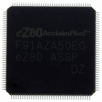
EZ80F91AZA50EG Zilog, EZ80F91AZA50EG Datasheet - Page 153

EZ80F91AZA50EG
Manufacturer Part Number
EZ80F91AZA50EG
Description
IC ACCLAIM MCU 256KB 144LQFP
Manufacturer
Zilog
Series
eZ80® AcclaimPlus!™r
Datasheet
1.EZ80F91AZA50SG.pdf
(387 pages)
Specifications of EZ80F91AZA50EG
Core Processor
Z8
Core Size
8-Bit
Speed
50MHz
Connectivity
Ethernet, I²C, IrDA, SPI, UART/USART
Peripherals
Brown-out Detect/Reset, POR, PWM, WDT
Number Of I /o
32
Program Memory Size
256KB (256K x 8)
Program Memory Type
FLASH
Ram Size
16K x 8
Voltage - Supply (vcc/vdd)
3 V ~ 3.6 V
Oscillator Type
Internal
Operating Temperature
-40°C ~ 105°C
Package / Case
144-LQFP
Processor Series
EZ80F91x
Core
eZ80
Data Bus Width
8 bit
Data Ram Size
16 KB
Interface Type
I2C, IrDA, SPI
Maximum Clock Frequency
50 MHz
Number Of Programmable I/os
32
Number Of Timers
4
Operating Supply Voltage
3 V to 3.6 V
Maximum Operating Temperature
+ 105 C
Mounting Style
SMD/SMT
Development Tools By Supplier
eZ80F910300ZCOG
Minimum Operating Temperature
- 40 C
For Use With
269-4712 - KIT DEV ENCORE 32 SERIES269-4671 - BOARD ZDOTS SBC Z80ACCLAIM PLUS269-4561 - KIT DEV FOR EZ80F91 W/C-COMPILER269-4560 - KIT DEV FOR EZ80F91 W/C-COMPILER
Lead Free Status / RoHS Status
Lead free / RoHS Compliant
Eeprom Size
-
Data Converters
-
Lead Free Status / Rohs Status
Details
Other names
269-4563
Available stocks
Company
Part Number
Manufacturer
Quantity
Price
- Current page: 153 of 387
- Download datasheet (5Mb)
PS027001-0707
Multi-PWM Mode
Timer Output Compare Value Register—High Byte
The Timer3 Output Compare x Value Register—High Byte (see
byte of the compare value for OC0–OC3.
Table 69. Compare Value Register—High Byte
TMR3_OC1_H = 0085h, TMR3_OC2_H = 0087h, TMR3_OC3_H = 0089h)
The special Multi-PWM mode uses the Timer 3 16-bit counter as the primary timekeeper
to control up to 4 PWM generators. The 16-bit reload value for Timer 3 sets a common
period for each of the PWM signals. However, the duty cycle and phase for each generator
are independent that is, the High and Low periods for each PWM generator are set inde-
pendently. In addition, each of the 4 PWM generators are enabled independently.
The 8 PWM signals (4 PWM output signals and their inverses) are output via Port A. A
functional block diagram of the Multi-PWM is illustrated in
Bit
Reset
CPU Access
Note: R/W = Read/Write.
Bit
Position
[7:0]
TMR3_OCx_H
Value
00h–FFh
R/W
7
0
Description
These bits represent the High byte of the 2-byte compare
value, {TMR3_OCx_H[7:0], TMR3_OCx_L[7:0]}. Bit 7 is bit
15 (msb) of the 16-bit data value. Bit 0 is bit 8
of the 16-bit timer compare value.
R/W
6
0
R/W
5
0
R/W
4
0
(TMR3_OC0_H = 0083h,
R/W
Figure 30
3
0
Programmable Reload Timers
Table
Product Specification
R/W
2
0
69) stores the High
on page 146.
eZ80F91 ASSP
R/W
1
0
R/W
0
0
145
Related parts for EZ80F91AZA50EG
Image
Part Number
Description
Manufacturer
Datasheet
Request
R

Part Number:
Description:
Communication Controllers, ZILOG INTELLIGENT PERIPHERAL CONTROLLER (ZIP)
Manufacturer:
Zilog, Inc.
Datasheet:

Part Number:
Description:
KIT DEV FOR Z8 ENCORE 16K TO 64K
Manufacturer:
Zilog
Datasheet:

Part Number:
Description:
KIT DEV Z8 ENCORE XP 28-PIN
Manufacturer:
Zilog
Datasheet:

Part Number:
Description:
DEV KIT FOR Z8 ENCORE 8K/4K
Manufacturer:
Zilog
Datasheet:

Part Number:
Description:
KIT DEV Z8 ENCORE XP 28-PIN
Manufacturer:
Zilog
Datasheet:

Part Number:
Description:
DEV KIT FOR Z8 ENCORE 4K TO 8K
Manufacturer:
Zilog
Datasheet:

Part Number:
Description:
CMOS Z8 microcontroller. ROM 16 Kbytes, RAM 256 bytes, speed 16 MHz, 32 lines I/O, 3.0V to 5.5V
Manufacturer:
Zilog, Inc.
Datasheet:

Part Number:
Description:
Low-cost microcontroller. 512 bytes ROM, 61 bytes RAM, 8 MHz
Manufacturer:
Zilog, Inc.
Datasheet:

Part Number:
Description:
Z8 4K OTP Microcontroller
Manufacturer:
Zilog, Inc.
Datasheet:

Part Number:
Description:
CMOS SUPER8 ROMLESS MCU
Manufacturer:
Zilog, Inc.
Datasheet:

Part Number:
Description:
SL1866 CMOSZ8 OTP Microcontroller
Manufacturer:
Zilog, Inc.
Datasheet:

Part Number:
Description:
SL1866 CMOSZ8 OTP Microcontroller
Manufacturer:
Zilog, Inc.
Datasheet:

Part Number:
Description:
OTP (KB) = 1, RAM = 125, Speed = 12, I/O = 14, 8-bit Timers = 2, Comm Interfaces Other Features = Por, LV Protect, Voltage = 4.5-5.5V
Manufacturer:
Zilog, Inc.
Datasheet:

Part Number:
Description:
Manufacturer:
Zilog, Inc.
Datasheet:


