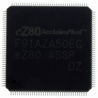
EZ80F91AZA50EG Zilog, EZ80F91AZA50EG Datasheet - Page 216

EZ80F91AZA50EG
Manufacturer Part Number
EZ80F91AZA50EG
Description
IC ACCLAIM MCU 256KB 144LQFP
Manufacturer
Zilog
Series
eZ80® AcclaimPlus!™r
Datasheet
1.EZ80F91AZA50SG.pdf
(387 pages)
Specifications of EZ80F91AZA50EG
Core Processor
Z8
Core Size
8-Bit
Speed
50MHz
Connectivity
Ethernet, I²C, IrDA, SPI, UART/USART
Peripherals
Brown-out Detect/Reset, POR, PWM, WDT
Number Of I /o
32
Program Memory Size
256KB (256K x 8)
Program Memory Type
FLASH
Ram Size
16K x 8
Voltage - Supply (vcc/vdd)
3 V ~ 3.6 V
Oscillator Type
Internal
Operating Temperature
-40°C ~ 105°C
Package / Case
144-LQFP
Processor Series
EZ80F91x
Core
eZ80
Data Bus Width
8 bit
Data Ram Size
16 KB
Interface Type
I2C, IrDA, SPI
Maximum Clock Frequency
50 MHz
Number Of Programmable I/os
32
Number Of Timers
4
Operating Supply Voltage
3 V to 3.6 V
Maximum Operating Temperature
+ 105 C
Mounting Style
SMD/SMT
Development Tools By Supplier
eZ80F910300ZCOG
Minimum Operating Temperature
- 40 C
For Use With
269-4712 - KIT DEV ENCORE 32 SERIES269-4671 - BOARD ZDOTS SBC Z80ACCLAIM PLUS269-4561 - KIT DEV FOR EZ80F91 W/C-COMPILER269-4560 - KIT DEV FOR EZ80F91 W/C-COMPILER
Lead Free Status / RoHS Status
Lead free / RoHS Compliant
Eeprom Size
-
Data Converters
-
Lead Free Status / Rohs Status
Details
Other names
269-4563
Available stocks
Company
Part Number
Manufacturer
Quantity
Price
- Current page: 216 of 387
- Download datasheet (5Mb)
PS027001-0707
Data Transfer Procedure with SPI Configured as a Slave
SPI Registers
1. Load the SPI BRG Registers, SPI_BRG_H and SPI_BRG_L. The external device
2. Load the SPI Control Register, SPI_CTL.
3. Assert the ENABLE pin of the slave device using a GPIO pin.
4. Load the SPI Transmit Shift Register, SPI_TSR.
5. When the SPI data transfer is complete, deassert the ENABLE pin of the slave device.
The following list describes the procedure for transferring data from a slave SPI device to
a master SPI device.
1. Load the SPI BRG Registers, SPI_BRG_H and SPI_BRG_L.
2. Load the SPI Transmit Shift Register, SPI_TSR. This load cannot occur while the SPI
3. Wait for the external SPI Master device to initiate the data transfer by asserting SS.
There are six registers in the Serial Peripheral Interface that provide control, status, and
data storage functions. The SPI registers are described in the following paragraphs.
SPI Baud Rate Generator Registers—Low Byte and High Byte
These registers hold the Low and High bytes of the 16-bit divisor count loaded by the CPU
for baud rate generation. The 16-bit clock divisor value is returned by {SPI_BRG_H,
SPI_BRG_L}. Upon RESET, the 16-bit BRG divisor value resets to
ured as a Master, the 16-bit divisor value must be between
When configured as a Slave, the 16-bit divisor value must be between
inclusive.
A Write to either the Low- or High-byte registers for the BRG Divisor Latch causes both
bytes to be loaded into the BRG counter and a restart of the count. See
Table 113
must deassert the SS pin if currently asserted.
slave is currently receiving data.
on page 209.
0003h
Product Specification
and
Serial Peripheral Interface
0002h
0004h
FFFFh
Table 112
eZ80F91 ASSP
. When config-
, inclusive.
and
and
FFFFh
,
208
Related parts for EZ80F91AZA50EG
Image
Part Number
Description
Manufacturer
Datasheet
Request
R

Part Number:
Description:
Communication Controllers, ZILOG INTELLIGENT PERIPHERAL CONTROLLER (ZIP)
Manufacturer:
Zilog, Inc.
Datasheet:

Part Number:
Description:
KIT DEV FOR Z8 ENCORE 16K TO 64K
Manufacturer:
Zilog
Datasheet:

Part Number:
Description:
KIT DEV Z8 ENCORE XP 28-PIN
Manufacturer:
Zilog
Datasheet:

Part Number:
Description:
DEV KIT FOR Z8 ENCORE 8K/4K
Manufacturer:
Zilog
Datasheet:

Part Number:
Description:
KIT DEV Z8 ENCORE XP 28-PIN
Manufacturer:
Zilog
Datasheet:

Part Number:
Description:
DEV KIT FOR Z8 ENCORE 4K TO 8K
Manufacturer:
Zilog
Datasheet:

Part Number:
Description:
CMOS Z8 microcontroller. ROM 16 Kbytes, RAM 256 bytes, speed 16 MHz, 32 lines I/O, 3.0V to 5.5V
Manufacturer:
Zilog, Inc.
Datasheet:

Part Number:
Description:
Low-cost microcontroller. 512 bytes ROM, 61 bytes RAM, 8 MHz
Manufacturer:
Zilog, Inc.
Datasheet:

Part Number:
Description:
Z8 4K OTP Microcontroller
Manufacturer:
Zilog, Inc.
Datasheet:

Part Number:
Description:
CMOS SUPER8 ROMLESS MCU
Manufacturer:
Zilog, Inc.
Datasheet:

Part Number:
Description:
SL1866 CMOSZ8 OTP Microcontroller
Manufacturer:
Zilog, Inc.
Datasheet:

Part Number:
Description:
SL1866 CMOSZ8 OTP Microcontroller
Manufacturer:
Zilog, Inc.
Datasheet:

Part Number:
Description:
OTP (KB) = 1, RAM = 125, Speed = 12, I/O = 14, 8-bit Timers = 2, Comm Interfaces Other Features = Por, LV Protect, Voltage = 4.5-5.5V
Manufacturer:
Zilog, Inc.
Datasheet:

Part Number:
Description:
Manufacturer:
Zilog, Inc.
Datasheet:


