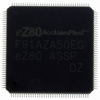
EZ80F91AZA50EG Zilog, EZ80F91AZA50EG Datasheet - Page 245

EZ80F91AZA50EG
Manufacturer Part Number
EZ80F91AZA50EG
Description
IC ACCLAIM MCU 256KB 144LQFP
Manufacturer
Zilog
Series
eZ80® AcclaimPlus!™r
Datasheet
1.EZ80F91AZA50SG.pdf
(387 pages)
Specifications of EZ80F91AZA50EG
Core Processor
Z8
Core Size
8-Bit
Speed
50MHz
Connectivity
Ethernet, I²C, IrDA, SPI, UART/USART
Peripherals
Brown-out Detect/Reset, POR, PWM, WDT
Number Of I /o
32
Program Memory Size
256KB (256K x 8)
Program Memory Type
FLASH
Ram Size
16K x 8
Voltage - Supply (vcc/vdd)
3 V ~ 3.6 V
Oscillator Type
Internal
Operating Temperature
-40°C ~ 105°C
Package / Case
144-LQFP
Processor Series
EZ80F91x
Core
eZ80
Data Bus Width
8 bit
Data Ram Size
16 KB
Interface Type
I2C, IrDA, SPI
Maximum Clock Frequency
50 MHz
Number Of Programmable I/os
32
Number Of Timers
4
Operating Supply Voltage
3 V to 3.6 V
Maximum Operating Temperature
+ 105 C
Mounting Style
SMD/SMT
Development Tools By Supplier
eZ80F910300ZCOG
Minimum Operating Temperature
- 40 C
For Use With
269-4712 - KIT DEV ENCORE 32 SERIES269-4671 - BOARD ZDOTS SBC Z80ACCLAIM PLUS269-4561 - KIT DEV FOR EZ80F91 W/C-COMPILER269-4560 - KIT DEV FOR EZ80F91 W/C-COMPILER
Lead Free Status / RoHS Status
Lead free / RoHS Compliant
Eeprom Size
-
Data Converters
-
Lead Free Status / Rohs Status
Details
Other names
269-4563
Available stocks
Company
Part Number
Manufacturer
Quantity
Price
- Current page: 245 of 387
- Download datasheet (5Mb)
PS027001-0707
ZDI Clock and Data Conventions
ZDI START Condition
The two pins used for communication with the ZDI block are the ZDI clock pin (ZCL) and
the ZDI data pin (ZDA). On eZ80F91, the ZCL pin is shared with the TCK pin while the
ZDA pin is shared with the TDI pin. The ZCL and ZDA pin functions are only available
when the On-Chip Instrumentation is disabled and the ZDI is therefore enabled. For gen-
eral data communication, the data value on the ZDA pin changes only when ZCL is Low
(0). The only exception is the ZDI START bit, which is indicated by a High-to-Low transi-
tion (falling edge) on the ZDA pin while ZCL is High.
Data is shifted into and out of ZDI, with the most-significant bit (bit 7) of each byte being
first in time, and the least-significant bit (bit 0) last in time. All information is passed
between the master and the slave in 8-bit (single-byte) units. Each byte is transferred with
nine clock cycles; eight to shift the data, and the ninth for internal operations.
All ZDI commands are preceded by the ZDI START signal, which is a High-to-Low tran-
sition of ZDA when ZCL is High. The ZDI slave on the eZ80F91 device continually mon-
itors the ZDA and ZCL lines for the START signal and does not respond to any command
until this condition is met. The master pulls ZDA Low, with ZCL High, to indicate the
beginning of a data transfer with the ZDI block.
trates a valid ZDI START signal prior to writing and reading data, respectively. A Low-to-
High transition of ZDA while the ZCL is High produces no effect.
Figure 49. Schematic For Building a Target Board ZPAK Connector
eZ80F91
TCK (ZCL)
TDI (ZDA)
10 Kohm
6-Pin Target Connector
10 Kohm
Figure 50
and
Figure
2
4
6
Product Specification
51on page 238 illus-
1
3
5
Zilog Debug Interface
eZ80F91 ASSP
(Target V
TV
DD
DD
)
237
Related parts for EZ80F91AZA50EG
Image
Part Number
Description
Manufacturer
Datasheet
Request
R

Part Number:
Description:
Communication Controllers, ZILOG INTELLIGENT PERIPHERAL CONTROLLER (ZIP)
Manufacturer:
Zilog, Inc.
Datasheet:

Part Number:
Description:
KIT DEV FOR Z8 ENCORE 16K TO 64K
Manufacturer:
Zilog
Datasheet:

Part Number:
Description:
KIT DEV Z8 ENCORE XP 28-PIN
Manufacturer:
Zilog
Datasheet:

Part Number:
Description:
DEV KIT FOR Z8 ENCORE 8K/4K
Manufacturer:
Zilog
Datasheet:

Part Number:
Description:
KIT DEV Z8 ENCORE XP 28-PIN
Manufacturer:
Zilog
Datasheet:

Part Number:
Description:
DEV KIT FOR Z8 ENCORE 4K TO 8K
Manufacturer:
Zilog
Datasheet:

Part Number:
Description:
CMOS Z8 microcontroller. ROM 16 Kbytes, RAM 256 bytes, speed 16 MHz, 32 lines I/O, 3.0V to 5.5V
Manufacturer:
Zilog, Inc.
Datasheet:

Part Number:
Description:
Low-cost microcontroller. 512 bytes ROM, 61 bytes RAM, 8 MHz
Manufacturer:
Zilog, Inc.
Datasheet:

Part Number:
Description:
Z8 4K OTP Microcontroller
Manufacturer:
Zilog, Inc.
Datasheet:

Part Number:
Description:
CMOS SUPER8 ROMLESS MCU
Manufacturer:
Zilog, Inc.
Datasheet:

Part Number:
Description:
SL1866 CMOSZ8 OTP Microcontroller
Manufacturer:
Zilog, Inc.
Datasheet:

Part Number:
Description:
SL1866 CMOSZ8 OTP Microcontroller
Manufacturer:
Zilog, Inc.
Datasheet:

Part Number:
Description:
OTP (KB) = 1, RAM = 125, Speed = 12, I/O = 14, 8-bit Timers = 2, Comm Interfaces Other Features = Por, LV Protect, Voltage = 4.5-5.5V
Manufacturer:
Zilog, Inc.
Datasheet:

Part Number:
Description:
Manufacturer:
Zilog, Inc.
Datasheet:


