MC9S08AC16CFJE Freescale Semiconductor, MC9S08AC16CFJE Datasheet - Page 168
MC9S08AC16CFJE
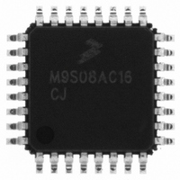
Manufacturer Part Number
MC9S08AC16CFJE
Description
IC MCU 8BIT 16K FLASH 32-LQFP
Manufacturer
Freescale Semiconductor
Series
HCS08r
Specifications of MC9S08AC16CFJE
Core Processor
HCS08
Core Size
8-Bit
Speed
40MHz
Connectivity
I²C, SCI, SPI
Peripherals
LVD, POR, PWM, WDT
Number Of I /o
22
Program Memory Size
16KB (16K x 8)
Program Memory Type
FLASH
Ram Size
1K x 8
Voltage - Supply (vcc/vdd)
2.7 V ~ 5.5 V
Data Converters
A/D 6x10b
Oscillator Type
Internal
Operating Temperature
-40°C ~ 85°C
Package / Case
32-LQFP
Processor Series
S08AC
Core
HCS08
Data Bus Width
8 bit
Data Ram Size
1 KB
Interface Type
SCI/SPI
Maximum Clock Frequency
40 MHz
Number Of Programmable I/os
22
Number Of Timers
8
Maximum Operating Temperature
+ 85 C
Mounting Style
SMD/SMT
3rd Party Development Tools
EWS08
Development Tools By Supplier
DEMO9S08AC60E, DEMOACEX, DEMOACKIT, DCF51AC256, DC9S08AC128, DC9S08AC16, DC9S08AC60, DEMO51AC256KIT
Minimum Operating Temperature
- 40 C
On-chip Adc
6-ch x 10-bit
Lead Free Status / RoHS Status
Lead free / RoHS Compliant
Eeprom Size
-
Lead Free Status / Rohs Status
Lead free / RoHS Compliant
Available stocks
Company
Part Number
Manufacturer
Quantity
Price

Company:
Part Number:
MC9S08AC16CFJE
Manufacturer:
Freescale Semiconductor
Quantity:
10 000
Company:
Part Number:
MC9S08AC16CFJER
Manufacturer:
Freescale Semiconductor
Quantity:
10 000


Timer/PWM Module (S08TPMV3)
10.4.1.1
Control bits in the timer status and control register allow the user to select nothing (timer disable), the
bus-rate clock (the normal default source), a crystal-related clock, or an external clock as the clock which
drives the TPM prescaler and subsequently the 16-bit TPM counter. The external clock source is
synchronized in the TPM. The bus clock clocks the synchronizer; the frequency of the external source must
be no more than one-fourth the frequency of the bus-rate clock, to meet Nyquist criteria and allowing for
jitter.
The external clock signal shares the same pin as a channel I/O pin, so the channel pin will not be usable
for channel I/O function when selected as the external clock source. It is the user’s responsibility to avoid
such settings. If this pin is used as an external clock source (CLKSB:CLKSA = 1:1), the channel can still
be used in output compare mode as a software timer (ELSnB:ELSnA = 0:0).
10.4.1.2
Each TPM channel is associated with an I/O pin on the MCU. The function of this pin depends on the
channel configuration. The TPM pins share with general purpose I/O pins, where each pin has a port data
register bit, and a data direction control bit, and the port has optional passive pullups which may be enabled
whenever a port pin is acting as an input.
The TPM channel does not control the I/O pin when (ELSnB:ELSnA = 0:0) or when (CLKSB:CLKSA =
0:0) so it normally reverts to general purpose I/O control. When CPWMS = 1 (and ELSnB:ELSnA not =
0:0), all channels within the TPM are configured for center-aligned PWM and the TPMxCHn pins are all
controlled by the TPM system. When CPWMS=0, the MSnB:MSnA control bits determine whether the
channel is configured for input capture, output compare, or edge-aligned PWM.
When a channel is configured for input capture (CPWMS=0, MSnB:MSnA = 0:0 and ELSnB:ELSnA not
= 0:0), the TPMxCHn pin is forced to act as an edge-sensitive input to the TPM. ELSnB:ELSnA control
bits determine what polarity edge or edges will trigger input-capture events. A synchronizer based on the
bus clock is used to synchronize input edges to the bus clock. This implies the minimum pulse width—that
can be reliably detected—on an input capture pin is four bus clock periods (with ideal clock pulses as near
as two bus clocks can be detected). TPM uses this pin as an input capture input to override the port data
and data direction controls for the same pin.
When a channel is configured for output compare (CPWMS=0, MSnB:MSnA = 0:1 and ELSnB:ELSnA
not = 0:0), the associated data direction control is overridden, the TPMxCHn pin is considered an output
controlled by the TPM, and the ELSnB:ELSnA control bits determine how the pin is controlled. The
remaining three combinations of ELSnB:ELSnA determine whether the TPMxCHn pin is toggled, cleared,
or set each time the 16-bit channel value register matches the timer counter.
When the output compare toggle mode is initially selected, the previous value on the pin is driven out until
the next output compare event—then the pin is toggled.
168
EXTCLK — External Clock Source
TPMxCHn — TPM Channel n I/O Pin(s)
MC9S08AC16 Series Data Sheet, Rev. 8
Freescale Semiconductor
Related parts for MC9S08AC16CFJE
Image
Part Number
Description
Manufacturer
Datasheet
Request
R

Part Number:
Description:
Manufacturer:
Freescale Semiconductor, Inc
Datasheet:
Part Number:
Description:
Manufacturer:
Freescale Semiconductor, Inc
Datasheet:
Part Number:
Description:
Manufacturer:
Freescale Semiconductor, Inc
Datasheet:
Part Number:
Description:
Manufacturer:
Freescale Semiconductor, Inc
Datasheet:
Part Number:
Description:
Manufacturer:
Freescale Semiconductor, Inc
Datasheet:
Part Number:
Description:
Manufacturer:
Freescale Semiconductor, Inc
Datasheet:
Part Number:
Description:
Manufacturer:
Freescale Semiconductor, Inc
Datasheet:
Part Number:
Description:
Manufacturer:
Freescale Semiconductor, Inc
Datasheet:
Part Number:
Description:
Manufacturer:
Freescale Semiconductor, Inc
Datasheet:
Part Number:
Description:
Manufacturer:
Freescale Semiconductor, Inc
Datasheet:
Part Number:
Description:
Manufacturer:
Freescale Semiconductor, Inc
Datasheet:
Part Number:
Description:
Manufacturer:
Freescale Semiconductor, Inc
Datasheet:
Part Number:
Description:
Manufacturer:
Freescale Semiconductor, Inc
Datasheet:
Part Number:
Description:
Manufacturer:
Freescale Semiconductor, Inc
Datasheet:
Part Number:
Description:
Manufacturer:
Freescale Semiconductor, Inc
Datasheet: