MC9S08AC16CFJE Freescale Semiconductor, MC9S08AC16CFJE Datasheet - Page 17
MC9S08AC16CFJE
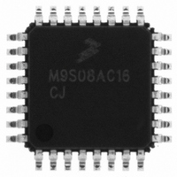
Manufacturer Part Number
MC9S08AC16CFJE
Description
IC MCU 8BIT 16K FLASH 32-LQFP
Manufacturer
Freescale Semiconductor
Series
HCS08r
Specifications of MC9S08AC16CFJE
Core Processor
HCS08
Core Size
8-Bit
Speed
40MHz
Connectivity
I²C, SCI, SPI
Peripherals
LVD, POR, PWM, WDT
Number Of I /o
22
Program Memory Size
16KB (16K x 8)
Program Memory Type
FLASH
Ram Size
1K x 8
Voltage - Supply (vcc/vdd)
2.7 V ~ 5.5 V
Data Converters
A/D 6x10b
Oscillator Type
Internal
Operating Temperature
-40°C ~ 85°C
Package / Case
32-LQFP
Processor Series
S08AC
Core
HCS08
Data Bus Width
8 bit
Data Ram Size
1 KB
Interface Type
SCI/SPI
Maximum Clock Frequency
40 MHz
Number Of Programmable I/os
22
Number Of Timers
8
Maximum Operating Temperature
+ 85 C
Mounting Style
SMD/SMT
3rd Party Development Tools
EWS08
Development Tools By Supplier
DEMO9S08AC60E, DEMOACEX, DEMOACKIT, DCF51AC256, DC9S08AC128, DC9S08AC16, DC9S08AC60, DEMO51AC256KIT
Minimum Operating Temperature
- 40 C
On-chip Adc
6-ch x 10-bit
Lead Free Status / RoHS Status
Lead free / RoHS Compliant
Eeprom Size
-
Lead Free Status / Rohs Status
Lead free / RoHS Compliant
Available stocks
Company
Part Number
Manufacturer
Quantity
Price

Company:
Part Number:
MC9S08AC16CFJE
Manufacturer:
Freescale Semiconductor
Quantity:
10 000
Company:
Part Number:
MC9S08AC16CFJER
Manufacturer:
Freescale Semiconductor
Quantity:
10 000


Section Number
14.6 Initialization Information ..............................................................................................................263
14.7 Application Information ................................................................................................................265
15.1 Introduction ...................................................................................................................................271
15.2 Background Debug Controller (BDC) ..........................................................................................272
15.3 On-Chip Debug System (DBG) ....................................................................................................281
15.4 Register Definition ........................................................................................................................285
A.1 Introduction ....................................................................................................................................293
A.2 Parameter Classification.................................................................................................................293
A.3 Absolute Maximum Ratings...........................................................................................................293
A.4 Thermal Characteristics..................................................................................................................294
A.5 ESD Protection and Latch-Up Immunity .......................................................................................296
A.6 DC Characteristics..........................................................................................................................297
A.7 Supply Current Characteristics.......................................................................................................301
A.8 ADC Characteristics.......................................................................................................................304
A.9 Internal Clock Generation Module Characteristics ........................................................................307
A.10 AC Characteristics..........................................................................................................................311
Freescale Semiconductor
14.5.7 MCU Stop3 Mode Operation ..........................................................................................262
14.5.8 MCU Stop1 and Stop2 Mode Operation .........................................................................263
14.6.1 ADC Module Initialization Example .............................................................................263
14.7.1 External Pins and Routing ..............................................................................................265
14.7.2 Sources of Error ..............................................................................................................267
15.1.1 Features ...........................................................................................................................272
15.2.1 BKGD Pin Description ...................................................................................................273
15.2.2 Communication Details ..................................................................................................274
15.2.3 BDC Commands .............................................................................................................278
15.2.4 BDC Hardware Breakpoint .............................................................................................280
15.3.1 Comparators A and B .....................................................................................................281
15.3.2 Bus Capture Information and FIFO Operation ...............................................................281
15.3.3 Change-of-Flow Information ..........................................................................................282
15.3.4 Tag vs. Force Breakpoints and Triggers .........................................................................282
15.3.5 Trigger Modes .................................................................................................................283
15.3.6 Hardware Breakpoints ....................................................................................................285
15.4.1 BDC Registers and Control Bits .....................................................................................285
15.4.2 System Background Debug Force Reset Register (SBDFR) ..........................................287
15.4.3 DBG Registers and Control Bits .....................................................................................288
A.9.1 ICG Frequency Specifications .........................................................................................308
Electrical Characteristics and Timing Specifications
MC9S08AC16 Series Data Sheet, Rev. 8
Development Support
Appendix A
Chapter 15
Title
Page
17
Related parts for MC9S08AC16CFJE
Image
Part Number
Description
Manufacturer
Datasheet
Request
R

Part Number:
Description:
Manufacturer:
Freescale Semiconductor, Inc
Datasheet:
Part Number:
Description:
Manufacturer:
Freescale Semiconductor, Inc
Datasheet:
Part Number:
Description:
Manufacturer:
Freescale Semiconductor, Inc
Datasheet:
Part Number:
Description:
Manufacturer:
Freescale Semiconductor, Inc
Datasheet:
Part Number:
Description:
Manufacturer:
Freescale Semiconductor, Inc
Datasheet:
Part Number:
Description:
Manufacturer:
Freescale Semiconductor, Inc
Datasheet:
Part Number:
Description:
Manufacturer:
Freescale Semiconductor, Inc
Datasheet:
Part Number:
Description:
Manufacturer:
Freescale Semiconductor, Inc
Datasheet:
Part Number:
Description:
Manufacturer:
Freescale Semiconductor, Inc
Datasheet:
Part Number:
Description:
Manufacturer:
Freescale Semiconductor, Inc
Datasheet:
Part Number:
Description:
Manufacturer:
Freescale Semiconductor, Inc
Datasheet:
Part Number:
Description:
Manufacturer:
Freescale Semiconductor, Inc
Datasheet:
Part Number:
Description:
Manufacturer:
Freescale Semiconductor, Inc
Datasheet:
Part Number:
Description:
Manufacturer:
Freescale Semiconductor, Inc
Datasheet:
Part Number:
Description:
Manufacturer:
Freescale Semiconductor, Inc
Datasheet: