COP8SAA716M8/NOPB National Semiconductor, COP8SAA716M8/NOPB Datasheet - Page 11
COP8SAA716M8/NOPB
Manufacturer Part Number
COP8SAA716M8/NOPB
Description
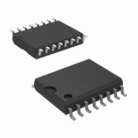
IC MCU OTP 8BIT 1K 16-SOIC
Manufacturer
National Semiconductor
Series
COP8™ 8SAr
Datasheet
1.COP8-PGMA-28CSP.pdf
(60 pages)
Specifications of COP8SAA716M8/NOPB
Core Processor
COP8
Core Size
8-Bit
Speed
10MHz
Connectivity
Microwire/Plus (SPI)
Peripherals
POR, PWM, WDT
Number Of I /o
12
Program Memory Size
1KB (1K x 8)
Program Memory Type
OTP
Ram Size
64 x 8
Voltage - Supply (vcc/vdd)
2.7 V ~ 5.5 V
Oscillator Type
Internal
Operating Temperature
-40°C ~ 85°C
Package / Case
16-SOIC (0.300", 7.5mm Width)
Package
16SOIC W
Family Name
COP8
Maximum Speed
10 MHz
Operating Supply Voltage
3.3|5 V
Data Bus Width
8 Bit
Interface Type
SPI
Number Of Timers
1
Maximum Clock Frequency
10 MHz
Data Ram Size
64 B
Number Of Programmable I/os
16
Height
2.3 mm
Length
10.5 mm
Maximum Operating Temperature
+ 85 C
Minimum Operating Temperature
- 40 C
Supply Voltage (max)
5.5 V
Supply Voltage (min)
2.7 V
Width
7.6 mm
Lead Free Status / RoHS Status
Lead free / RoHS Compliant
Eeprom Size
-
Data Converters
-
Lead Free Status / Rohs Status
Details
Other names
*COP8SAA716M8
*COP8SAA716M8/NOPB
COP8SAA716M8
*COP8SAA716M8/NOPB
COP8SAA716M8
Available stocks
Company
Part Number
Manufacturer
Quantity
Price
Company:

Part Number:
COP8SAA716M8/NOPB
Manufacturer:
ADI
Quantity:
51


Inputs
Output Propagation Delay (Note 16)
MICROWIRE Setup Time (t
MICROWIRE Hold Time (t
MICROWIRE Output Propagation Delay (t
MICROWIRE Maximum Shift Clock
Input Pulse Width (Note 17)
Reset Pulse Width
AC Electrical Characteristics
Note 11: t
Note 12: Maximum rate of voltage change must be
Note 13: Supply and IDLE currents are measured with CKI driven with a square wave Oscillator, CKO driven 180˚ out of phase with CKI, inputs connected to V
and outputs driven low but not connected to a load.
Note 14: The HALT mode will stop CKI from oscillating in the R/C and the Crystal configurations. In the R/C configuration, CKI is forced high internally. In the crystal
or external configuration, CKI is TRI-STATE. Measurement of I
programmed as low outputs and not driving a load; all outputs programmed low and not driving a load; all inputs tied to V
to HALT mode entered via setting bit 7 of the G Port data register.
Note 15: Pins G6 and RESET are designed with a high voltage input network. These pins allow input voltages
biased at voltages
pins will not latch up. The voltage at the pins must be limited to
ESD transients.
Note 16: The output propagation delay is referenced to the end of the instruction cycle where the output change occurs.
Note 17: Parameter characterized but not tested.
Note 18: Rise times faster than this specification may reset the device if POR is enabled and may affect the value of Idle Timer T0 if POR is not enabled.
−40˚C
t
t
t
SO, SK
All Others
Master Mode
Slave Mode
Interrupt Input High Time
Interrupt Input Low Time
Timer 1 Input High Time
Timer 1 Input Low Time
SETUP
HOLD
PD1
, t
PD0
C
T
= Instruction cycle time (Clock input frequency divided by 10).
A
+85˚C unless otherwise specified.
>
Parameter
V
CC
(the pins do not have source current when biased at a voltage below V
UWH
UWS
) (Note 16)
) (Note 16)
UPD
<
0.5 V/ms.
FIGURE 4. MICROWIRE/PLUS Timing
)
4.5V
2.7V
4.5V
2.7V
R
4.5V
2.7V
4.5V
2.7V
(Continued)
<
DD
L
14V. WARNING: Voltages in excess of 14V will cause damage to the pins. This warning excludes
= 2.2k, C
HALT is done with device neither sourcing nor sinking current; with L. F, C, G0, and G2–G5
V
V
V
V
V
V
V
V
Conditions
CC
CC
CC
CC
CC
CC
CC
CC
<
<
<
<
L
11
5.5V
5.5V
5.5V
5.5V
4.5V
4.5V
= 100 pF
4.5V
4.5V
CC
). The effective resistance to V
DS012838-9
Min
200
500
150
60
20
56
1
1
1
1
1
>
V
CC
and the pins will have sink current to V
CC
; clock monitor disabled. Parameter refers
Typ
CC
is 750
Max
1.75
220
500
0.7
1.0
2.5
1
(typical). These two
www.national.com
Units
CC
MHz
kHz
ns
ns
ns
ns
µs
µs
µs
µs
ns
ns
ns
µs
t
t
t
t
C
C
C
C
when
CC
Related parts for COP8SAA716M8/NOPB
Image
Part Number
Description
Manufacturer
Datasheet
Request
R

Part Number:
Description:
National Semiconductor [8-Bit D/A Converter]
Manufacturer:
National Semiconductor
Datasheet:
Part Number:
Description:
National Semiconductor [Media Coprocessor]
Manufacturer:
National Semiconductor
Datasheet:
Part Number:
Description:
Digitally Controlled Tone and Volume Circuit with Stereo Audio Power Amplifier, Microphone Preamp Stage and National 3D Sound
Manufacturer:
National Semiconductor
Datasheet:
Part Number:
Description:
Digitally Controlled Tone and Volume Circuit with Stereo Audio Power Amplifier, Microphone Preamp Stage and National 3D Sound
Manufacturer:
National Semiconductor
Datasheet:
Part Number:
Description:
AC97 Rev 2 Codec with Sample Rate Conversion and National 3D Sound
Manufacturer:
National Semiconductor
Part Number:
Description:
Manufacturer:
National Semiconductor
Datasheet:
Part Number:
Description:
Manufacturer:
National Semiconductor
Datasheet:
Part Number:
Description:
General Purpose, Low Voltage, Low Power, Rail-to-Rail Output Operational Amplifiers
Manufacturer:
National Semiconductor
Datasheet:
Part Number:
Description:
8-bit 20 MSPS flash A/D converter.
Manufacturer:
National Semiconductor
Datasheet:
Part Number:
Description:
Low Noise Quad Operational Amplifier
Manufacturer:
National Semiconductor
Datasheet:
Part Number:
Description:
Quad Differential Line Receivers
Manufacturer:
National Semiconductor
Datasheet:
Part Number:
Description:
Quad High Speed Trapezoidal? Bus Transceiver
Manufacturer:
National Semiconductor
Datasheet:
Part Number:
Description:
Dual Line Receiver
Manufacturer:
National Semiconductor
Datasheet:
Part Number:
Description:
TTL to 10k ECL Level Translator with Latch
Manufacturer:
National Semiconductor
Datasheet: