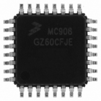
MC908GZ60CFJE Freescale Semiconductor, MC908GZ60CFJE Datasheet - Page 167

MC908GZ60CFJE
Manufacturer Part Number
MC908GZ60CFJE
Description
IC MCU 60K FLASH 8MHZ 32-LQFP
Manufacturer
Freescale Semiconductor
Series
HC08r
Datasheet
1.MC908GZ60CFJE.pdf
(352 pages)
Specifications of MC908GZ60CFJE
Core Processor
HC08
Core Size
8-Bit
Speed
8MHz
Connectivity
CAN, SCI, SPI
Peripherals
LVD, POR, PWM
Number Of I /o
21
Program Memory Size
60KB (60K x 8)
Program Memory Type
FLASH
Ram Size
2K x 8
Voltage - Supply (vcc/vdd)
3 V ~ 5.5 V
Data Converters
A/D 24x10b
Oscillator Type
Internal
Operating Temperature
-40°C ~ 85°C
Package / Case
32-LQFP
Controller Family/series
HC08
No. Of I/o's
21
Ram Memory Size
2KB
Cpu Speed
8MHz
No. Of Timers
2
Embedded Interface Type
CAN, SCI, SPI
Rohs Compliant
Yes
Processor Series
HC08GZ
Core
HC08
Data Bus Width
8 bit
Data Ram Size
2 KB
Interface Type
CAN, ESCI, SPI
Maximum Clock Frequency
8 MHz
Number Of Programmable I/os
53
Number Of Timers
8
Maximum Operating Temperature
+ 85 C
Mounting Style
SMD/SMT
Development Tools By Supplier
FSICEBASE, DEMO908GZ60E, M68EML08GZE
Minimum Operating Temperature
- 40 C
On-chip Adc
10 bit, 24 Channel
Lead Free Status / RoHS Status
Lead free / RoHS Compliant
Eeprom Size
-
Lead Free Status / Rohs Status
Details
Available stocks
Company
Part Number
Manufacturer
Quantity
Price
Company:
Part Number:
MC908GZ60CFJE
Manufacturer:
Freescale
Quantity:
4 000
Company:
Part Number:
MC908GZ60CFJE
Manufacturer:
Freescale Semiconductor
Quantity:
10 000
- Current page: 167 of 352
- Download datasheet (5Mb)
AC7–AC0 — Acceptance Code Bits
12.13.13 MSCAN08 Identifier Mask Registers (CIDMR0–CIDMR3)
The identifier mask registers specify which of the corresponding bits in the identifier acceptance register
are relevant for acceptance filtering. For standard identifiers it is required to program the last three bits
(AM2–AM0) in the mask register CIDMR1 to ‘don’t care’.
AM7–AM0 — Acceptance Mask Bits
Freescale Semiconductor
AC7–AC0 comprise a user-defined sequence of bits with which the corresponding bits of the related
identifier register (IDRn) of the receive message buffer are compared. The result of this comparison is
then masked with the corresponding identifier mask register.
If a particular bit in this register is cleared, this indicates that the corresponding bit in the identifier
acceptance register must be the same as its identifier bit before a match will be detected. The message
will be accepted if all such bits match. If a bit is set, it indicates that the state of the corresponding bit
in the identifier acceptance register will not affect whether or not the message is accepted.
1 = Ignore corresponding acceptance code register bit.
0 = Match corresponding acceptance code register and identifier bits.
CIDMRO Address: $0514
CIDMR1 Address: $0515
CIDMR2 Address: $0516
CIDMR3 Address: $0517
The CIDAR0–CIDAR3 registers can be written only if the SFTRES bit in
CMCR0 is set
The CIDMR0–CIDMR3 registers can be written only if the SFTRES bit in
the CMCR0 is set
Reset:
Reset:
Reset:
Reset:
Read:
Read:
Read:
Read:
Write:
Write:
Write:
Write:
MC68HC908GZ60 • MC68HC908GZ48 • MC68HC908GZ32 Data Sheet, Rev. 6
AM7
AM7
AM7
AM7
Bit 7
Bit 7
Bit 7
Bit 7
Figure 12-28. Identifier Mask Registers
AM6
AM6
AM6
AM6
6
6
6
6
AM5
AM5
AM5
AM5
(CIDMR0–CIDMR3)
5
5
5
5
NOTE
NOTE
Unaffected by reset
Unaffected by reset
Unaffected by reset
Unaffected by reset
AM4
AM4
AM4
AM4
4
4
4
4
AM3
AM3
AM3
AM3
3
3
3
3
Programmer’s Model of Control Registers
AM2
AM2
AM2
AM2
2
2
2
2
AM1
AM1
AM1
AM1
1
1
1
1
Bit 0
AM0
Bit 0
AM0
Bit 0
AM0
Bit 0
AM0
167
Related parts for MC908GZ60CFJE
Image
Part Number
Description
Manufacturer
Datasheet
Request
R
Part Number:
Description:
Manufacturer:
Freescale Semiconductor, Inc
Datasheet:
Part Number:
Description:
Manufacturer:
Freescale Semiconductor, Inc
Datasheet:
Part Number:
Description:
Manufacturer:
Freescale Semiconductor, Inc
Datasheet:
Part Number:
Description:
Manufacturer:
Freescale Semiconductor, Inc
Datasheet:
Part Number:
Description:
Manufacturer:
Freescale Semiconductor, Inc
Datasheet:
Part Number:
Description:
Manufacturer:
Freescale Semiconductor, Inc
Datasheet:
Part Number:
Description:
Manufacturer:
Freescale Semiconductor, Inc
Datasheet:
Part Number:
Description:
Manufacturer:
Freescale Semiconductor, Inc
Datasheet:
Part Number:
Description:
Manufacturer:
Freescale Semiconductor, Inc
Datasheet:
Part Number:
Description:
Manufacturer:
Freescale Semiconductor, Inc
Datasheet:
Part Number:
Description:
Manufacturer:
Freescale Semiconductor, Inc
Datasheet:
Part Number:
Description:
Manufacturer:
Freescale Semiconductor, Inc
Datasheet:
Part Number:
Description:
Manufacturer:
Freescale Semiconductor, Inc
Datasheet:
Part Number:
Description:
Manufacturer:
Freescale Semiconductor, Inc
Datasheet:
Part Number:
Description:
Manufacturer:
Freescale Semiconductor, Inc
Datasheet:


