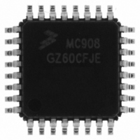
MC908GZ60CFJE Freescale Semiconductor, MC908GZ60CFJE Datasheet - Page 169

MC908GZ60CFJE
Manufacturer Part Number
MC908GZ60CFJE
Description
IC MCU 60K FLASH 8MHZ 32-LQFP
Manufacturer
Freescale Semiconductor
Series
HC08r
Datasheet
1.MC908GZ60CFJE.pdf
(352 pages)
Specifications of MC908GZ60CFJE
Core Processor
HC08
Core Size
8-Bit
Speed
8MHz
Connectivity
CAN, SCI, SPI
Peripherals
LVD, POR, PWM
Number Of I /o
21
Program Memory Size
60KB (60K x 8)
Program Memory Type
FLASH
Ram Size
2K x 8
Voltage - Supply (vcc/vdd)
3 V ~ 5.5 V
Data Converters
A/D 24x10b
Oscillator Type
Internal
Operating Temperature
-40°C ~ 85°C
Package / Case
32-LQFP
Controller Family/series
HC08
No. Of I/o's
21
Ram Memory Size
2KB
Cpu Speed
8MHz
No. Of Timers
2
Embedded Interface Type
CAN, SCI, SPI
Rohs Compliant
Yes
Processor Series
HC08GZ
Core
HC08
Data Bus Width
8 bit
Data Ram Size
2 KB
Interface Type
CAN, ESCI, SPI
Maximum Clock Frequency
8 MHz
Number Of Programmable I/os
53
Number Of Timers
8
Maximum Operating Temperature
+ 85 C
Mounting Style
SMD/SMT
Development Tools By Supplier
FSICEBASE, DEMO908GZ60E, M68EML08GZE
Minimum Operating Temperature
- 40 C
On-chip Adc
10 bit, 24 Channel
Lead Free Status / RoHS Status
Lead free / RoHS Compliant
Eeprom Size
-
Lead Free Status / Rohs Status
Details
Available stocks
Company
Part Number
Manufacturer
Quantity
Price
Company:
Part Number:
MC908GZ60CFJE
Manufacturer:
Freescale
Quantity:
4 000
Company:
Part Number:
MC908GZ60CFJE
Manufacturer:
Freescale Semiconductor
Quantity:
10 000
- Current page: 169 of 352
- Download datasheet (5Mb)
Chapter 13
Input/Output (I/O) Ports
13.1 Introduction
Bidirectional input-output (I/O) pins form seven parallel ports. All I/O pins are programmable as inputs or
outputs. All individual bits within port A, port C, port D and port F are software configurable with pullup
devices if configured as input port bits. The pullup devices are automatically and dynamically disabled
when a port bit is switched to output mode.
13.2 Unused Pin Termination
Input pins and I/O port pins that are not used in the application must be terminated. This prevents excess
current caused by floating inputs, and enhances immunity during noise or transient events. Termination
methods include:
Never connect unused pins directly to V
Since some general-purpose I/O pins are not available on all packages, these pins must be terminated
as well. Either method 1 or 2 above are appropriate.
Freescale Semiconductor
Addr.
$0000
$0001
$0002
$0003
1. Configuring unused pins as outputs and driving high or low;
2. Configuring unused pins as inputs and enabling internal pull-ups;
3. Configuring unused pins as inputs and using external pull-up or pull-down resistors.
Register Name
Port A Data Register
Port B Data Register
Port C Data Register
Port D Data Register
See page 173.
See page 176.
See page 178.
See page 180.
MC68HC908GZ60 • MC68HC908GZ48 • MC68HC908GZ32 Data Sheet, Rev. 6
(PTC)
(PTD)
(PTA)
(PTB)
Figure 13-1. I/O Port Register Summary (Sheet 1 of 3)
Reset:
Reset:
Reset:
Reset:
Read:
Read:
Read:
Read:
Write:
Write:
Write:
Write:
PTD7
PTA7
PTB7
Bit 7
1
DD
= Unimplemented
or V
PTC6
PTD6
PTA6
PTB6
6
SS
.
PTC5
PTD5
PTA5
PTB5
5
Unaffected by reset
Unaffected by reset
Unaffected by reset
Unaffected by reset
PTA4
PTB4
PTC4
PTD4
4
PTA3
PTB3
PTC3
PTD3
3
PTA2
PTB2
PTC2
PTD2
2
PTA1
PTB1
PTC1
PTD1
1
PTA0
PTB0
PTC0
PTD0
Bit 0
169
Related parts for MC908GZ60CFJE
Image
Part Number
Description
Manufacturer
Datasheet
Request
R
Part Number:
Description:
Manufacturer:
Freescale Semiconductor, Inc
Datasheet:
Part Number:
Description:
Manufacturer:
Freescale Semiconductor, Inc
Datasheet:
Part Number:
Description:
Manufacturer:
Freescale Semiconductor, Inc
Datasheet:
Part Number:
Description:
Manufacturer:
Freescale Semiconductor, Inc
Datasheet:
Part Number:
Description:
Manufacturer:
Freescale Semiconductor, Inc
Datasheet:
Part Number:
Description:
Manufacturer:
Freescale Semiconductor, Inc
Datasheet:
Part Number:
Description:
Manufacturer:
Freescale Semiconductor, Inc
Datasheet:
Part Number:
Description:
Manufacturer:
Freescale Semiconductor, Inc
Datasheet:
Part Number:
Description:
Manufacturer:
Freescale Semiconductor, Inc
Datasheet:
Part Number:
Description:
Manufacturer:
Freescale Semiconductor, Inc
Datasheet:
Part Number:
Description:
Manufacturer:
Freescale Semiconductor, Inc
Datasheet:
Part Number:
Description:
Manufacturer:
Freescale Semiconductor, Inc
Datasheet:
Part Number:
Description:
Manufacturer:
Freescale Semiconductor, Inc
Datasheet:
Part Number:
Description:
Manufacturer:
Freescale Semiconductor, Inc
Datasheet:
Part Number:
Description:
Manufacturer:
Freescale Semiconductor, Inc
Datasheet:


