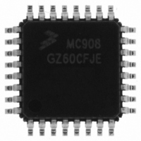
MC908GZ60CFJE Freescale Semiconductor, MC908GZ60CFJE Datasheet - Page 47

MC908GZ60CFJE
Manufacturer Part Number
MC908GZ60CFJE
Description
IC MCU 60K FLASH 8MHZ 32-LQFP
Manufacturer
Freescale Semiconductor
Series
HC08r
Datasheet
1.MC908GZ60CFJE.pdf
(352 pages)
Specifications of MC908GZ60CFJE
Core Processor
HC08
Core Size
8-Bit
Speed
8MHz
Connectivity
CAN, SCI, SPI
Peripherals
LVD, POR, PWM
Number Of I /o
21
Program Memory Size
60KB (60K x 8)
Program Memory Type
FLASH
Ram Size
2K x 8
Voltage - Supply (vcc/vdd)
3 V ~ 5.5 V
Data Converters
A/D 24x10b
Oscillator Type
Internal
Operating Temperature
-40°C ~ 85°C
Package / Case
32-LQFP
Controller Family/series
HC08
No. Of I/o's
21
Ram Memory Size
2KB
Cpu Speed
8MHz
No. Of Timers
2
Embedded Interface Type
CAN, SCI, SPI
Rohs Compliant
Yes
Processor Series
HC08GZ
Core
HC08
Data Bus Width
8 bit
Data Ram Size
2 KB
Interface Type
CAN, ESCI, SPI
Maximum Clock Frequency
8 MHz
Number Of Programmable I/os
53
Number Of Timers
8
Maximum Operating Temperature
+ 85 C
Mounting Style
SMD/SMT
Development Tools By Supplier
FSICEBASE, DEMO908GZ60E, M68EML08GZE
Minimum Operating Temperature
- 40 C
On-chip Adc
10 bit, 24 Channel
Lead Free Status / RoHS Status
Lead free / RoHS Compliant
Eeprom Size
-
Lead Free Status / Rohs Status
Details
Available stocks
Company
Part Number
Manufacturer
Quantity
Price
Company:
Part Number:
MC908GZ60CFJE
Manufacturer:
Freescale
Quantity:
4 000
Company:
Part Number:
MC908GZ60CFJE
Manufacturer:
Freescale Semiconductor
Quantity:
10 000
- Current page: 47 of 352
- Download datasheet (5Mb)
2.6.2.2 FLASH-1 Block Protect Register
The FLASH-1 block protect register (FL1BPR) is implemented as a byte within the FLASH-1 memory;
therefore, it can only be written during a FLASH programming sequence. The value in this register
determines the starting location of the protected range within the FLASH-1 memory.
FL1BPR[7:0] — Block Protect Register Bits 7 to 0
Decreasing the value in FL1BPR by one increases the protected range by one page (128 bytes).
However, programming the block protect register with $FE protects a range twice that size, 256 bytes, in
the corresponding array. $FE means that locations $FF00–$FFFF are protected in FLASH-1.
The FLASH memory does not exist at some locations. The block protection range configuration is
unaffected if FLASH memory does not exist in that range. Refer to
desired locations are protected.
Freescale Semiconductor
These eight bits represent bits [14:7] of a 16-bit memory address. Bit 15 is a 1 and bits [6:0] are 0s.
The resultant 16-bit address is used for specifying the start address of the FLASH-1 memory for block
protection. FLASH-1 is protected from this start address to the end of FLASH-1 memory at $FFFF.
With this mechanism, the protect start address can be $XX00 and $XX80 (128 byte page boundaries)
within the FLASH-1 array.
Address: $FF80
Read:
Write:
START ADDRESS OF FLASH
MC68HC908GZ60 • MC68HC908GZ48 • MC68HC908GZ32 Data Sheet, Rev. 6
Figure 2-4. FLASH-1 Block Protect Register (FL1BPR)
BPR7
Bit 7
BLOCK PROTECT
Figure 2-5. FLASH-1 Block Protect Start Address
FL1BPR[7:0]
$FF
$FE
$FD
$0B
$0A
Table 2-2. FLASH-1 Protected Ranges
$09
$08
$04
$03
$02
$01
$00
BPR6
↓
↓
6
1
BPR5
5
FLBPR VALUE
16-BIT MEMORY ADDRESS
Unaffected by reset
BPR4
4
Protected Range
$FF00–$FFFF
$FE80–$FFFF
$8580–$FFFF
$8500–$FFFF
$8480–$FFFF
$8400–$FFFF
$8200–$FFFF
$8180–$FFFF
$8100–$FFFF
$8080–$FFFF
$8000–$FFFF
No protection
BPR3
3
↓
↓
0 0 0 0 0 0 0
Figure 2-1
BPR2
2
BPR1
and make sure that the
1
FLASH-1 Memory (FLASH-1)
BPR0
Bit 0
47
Related parts for MC908GZ60CFJE
Image
Part Number
Description
Manufacturer
Datasheet
Request
R
Part Number:
Description:
Manufacturer:
Freescale Semiconductor, Inc
Datasheet:
Part Number:
Description:
Manufacturer:
Freescale Semiconductor, Inc
Datasheet:
Part Number:
Description:
Manufacturer:
Freescale Semiconductor, Inc
Datasheet:
Part Number:
Description:
Manufacturer:
Freescale Semiconductor, Inc
Datasheet:
Part Number:
Description:
Manufacturer:
Freescale Semiconductor, Inc
Datasheet:
Part Number:
Description:
Manufacturer:
Freescale Semiconductor, Inc
Datasheet:
Part Number:
Description:
Manufacturer:
Freescale Semiconductor, Inc
Datasheet:
Part Number:
Description:
Manufacturer:
Freescale Semiconductor, Inc
Datasheet:
Part Number:
Description:
Manufacturer:
Freescale Semiconductor, Inc
Datasheet:
Part Number:
Description:
Manufacturer:
Freescale Semiconductor, Inc
Datasheet:
Part Number:
Description:
Manufacturer:
Freescale Semiconductor, Inc
Datasheet:
Part Number:
Description:
Manufacturer:
Freescale Semiconductor, Inc
Datasheet:
Part Number:
Description:
Manufacturer:
Freescale Semiconductor, Inc
Datasheet:
Part Number:
Description:
Manufacturer:
Freescale Semiconductor, Inc
Datasheet:
Part Number:
Description:
Manufacturer:
Freescale Semiconductor, Inc
Datasheet:


