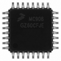
MC908GZ60CFJE Freescale Semiconductor, MC908GZ60CFJE Datasheet - Page 61

MC908GZ60CFJE
Manufacturer Part Number
MC908GZ60CFJE
Description
IC MCU 60K FLASH 8MHZ 32-LQFP
Manufacturer
Freescale Semiconductor
Series
HC08r
Datasheet
1.MC908GZ60CFJE.pdf
(352 pages)
Specifications of MC908GZ60CFJE
Core Processor
HC08
Core Size
8-Bit
Speed
8MHz
Connectivity
CAN, SCI, SPI
Peripherals
LVD, POR, PWM
Number Of I /o
21
Program Memory Size
60KB (60K x 8)
Program Memory Type
FLASH
Ram Size
2K x 8
Voltage - Supply (vcc/vdd)
3 V ~ 5.5 V
Data Converters
A/D 24x10b
Oscillator Type
Internal
Operating Temperature
-40°C ~ 85°C
Package / Case
32-LQFP
Controller Family/series
HC08
No. Of I/o's
21
Ram Memory Size
2KB
Cpu Speed
8MHz
No. Of Timers
2
Embedded Interface Type
CAN, SCI, SPI
Rohs Compliant
Yes
Processor Series
HC08GZ
Core
HC08
Data Bus Width
8 bit
Data Ram Size
2 KB
Interface Type
CAN, ESCI, SPI
Maximum Clock Frequency
8 MHz
Number Of Programmable I/os
53
Number Of Timers
8
Maximum Operating Temperature
+ 85 C
Mounting Style
SMD/SMT
Development Tools By Supplier
FSICEBASE, DEMO908GZ60E, M68EML08GZE
Minimum Operating Temperature
- 40 C
On-chip Adc
10 bit, 24 Channel
Lead Free Status / RoHS Status
Lead free / RoHS Compliant
Eeprom Size
-
Lead Free Status / Rohs Status
Details
Available stocks
Company
Part Number
Manufacturer
Quantity
Price
Company:
Part Number:
MC908GZ60CFJE
Manufacturer:
Freescale
Quantity:
4 000
Company:
Part Number:
MC908GZ60CFJE
Manufacturer:
Freescale Semiconductor
Quantity:
10 000
- Current page: 61 of 352
- Download datasheet (5Mb)
Chapter 3
Analog-to-Digital Converter (ADC)
3.1 Introduction
This section describes the 10-bit analog-to-digital converter (ADC).
3.2 Features
Features of the ADC module include:
3.3 Functional Description
The ADC provides 24 pins for sampling external sources at pins PTG7/AD23–PTG0/AD16,
PTA7/KBD7/AD15–PTA0/KBD0/AD8, and PTB7/AD7–PTB0/AD0. An analog multiplexer allows the
single ADC converter to select one of 24 ADC channels as ADC voltage in (V
the successive approximation register-based analog-to-digital converter. When the conversion is
completed, ADC places the result in the ADC data register and sets a flag or generates an interrupt. See
Figure
3.3.1 ADC Port I/O Pins
PTG7/AD23–PTG0/AD16, PTA7/KBD7/AD15–PTA0/KBD0/AD8, and PTB7/AD7–PTB0/AD0 are
general-purpose I/O (input/output) pins that share with the ADC channels. The channel select bits define
which ADC channel/port pin will be used as the input signal. The ADC overrides the port I/O logic by
forcing that pin as input to the ADC. The remaining ADC channels/port pins are controlled by the port I/O
logic and can be used as general-purpose I/O. Writes to the port register or data direction register (DDR)
will not have any affect on the port pin that is selected by the ADC. A read of a port pin in use by the ADC
will return a 0.
Freescale Semiconductor
•
•
•
•
•
•
•
•
24 channels with multiplexed input
Linear successive approximation with monotonicity
10-bit resolution
Single or continuous conversion
Conversion complete flag or conversion complete interrupt
Selectable ADC clock
Left or right justified result
Left justified sign data mode
3-2.
MC68HC908GZ60 • MC68HC908GZ48 • MC68HC908GZ32 Data Sheet, Rev. 6
ADIN
). V
ADIN
is converted by
61
Related parts for MC908GZ60CFJE
Image
Part Number
Description
Manufacturer
Datasheet
Request
R
Part Number:
Description:
Manufacturer:
Freescale Semiconductor, Inc
Datasheet:
Part Number:
Description:
Manufacturer:
Freescale Semiconductor, Inc
Datasheet:
Part Number:
Description:
Manufacturer:
Freescale Semiconductor, Inc
Datasheet:
Part Number:
Description:
Manufacturer:
Freescale Semiconductor, Inc
Datasheet:
Part Number:
Description:
Manufacturer:
Freescale Semiconductor, Inc
Datasheet:
Part Number:
Description:
Manufacturer:
Freescale Semiconductor, Inc
Datasheet:
Part Number:
Description:
Manufacturer:
Freescale Semiconductor, Inc
Datasheet:
Part Number:
Description:
Manufacturer:
Freescale Semiconductor, Inc
Datasheet:
Part Number:
Description:
Manufacturer:
Freescale Semiconductor, Inc
Datasheet:
Part Number:
Description:
Manufacturer:
Freescale Semiconductor, Inc
Datasheet:
Part Number:
Description:
Manufacturer:
Freescale Semiconductor, Inc
Datasheet:
Part Number:
Description:
Manufacturer:
Freescale Semiconductor, Inc
Datasheet:
Part Number:
Description:
Manufacturer:
Freescale Semiconductor, Inc
Datasheet:
Part Number:
Description:
Manufacturer:
Freescale Semiconductor, Inc
Datasheet:
Part Number:
Description:
Manufacturer:
Freescale Semiconductor, Inc
Datasheet:


