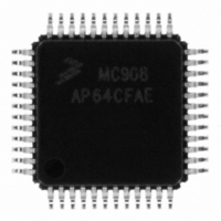
MC908AP64CFAE Freescale Semiconductor, MC908AP64CFAE Datasheet - Page 241

MC908AP64CFAE
Manufacturer Part Number
MC908AP64CFAE
Description
IC MCU 64K 8MHZ SPI 48-LQFP
Manufacturer
Freescale Semiconductor
Series
HC08r
Specifications of MC908AP64CFAE
Core Processor
HC08
Core Size
8-Bit
Speed
8MHz
Connectivity
I²C, IRSCI, SCI, SPI
Peripherals
LED, LVD, POR, PWM
Number Of I /o
32
Program Memory Size
64KB (64K x 8)
Program Memory Type
FLASH
Ram Size
2K x 8
Voltage - Supply (vcc/vdd)
2.7 V ~ 5.5 V
Data Converters
A/D 8x10b
Oscillator Type
Internal
Operating Temperature
-40°C ~ 85°C
Package / Case
48-LQFP
Cpu Family
HC08
Device Core Size
8b
Frequency (max)
8MHz
Interface Type
SCI/SPI
Total Internal Ram Size
2KB
# I/os (max)
32
Number Of Timers - General Purpose
4
Operating Supply Voltage (typ)
3.3/5V
Operating Supply Voltage (max)
5.5V
Operating Supply Voltage (min)
2.7V
On-chip Adc
8-chx10-bit
Instruction Set Architecture
CISC
Operating Temp Range
-40C to 85C
Operating Temperature Classification
Industrial
Mounting
Surface Mount
Pin Count
48
Package Type
LQFP
Controller Family/series
HC08
No. Of I/o's
32
Ram Memory Size
2KB
Cpu Speed
8MHz
No. Of Timers
2
Embedded Interface Type
I2C, SCI, SPI
Rohs Compliant
Yes
Processor Series
HC08AP
Core
HC08
Data Bus Width
8 bit
Data Ram Size
2 KB
Maximum Clock Frequency
8 MHz
Number Of Programmable I/os
32
Number Of Timers
4
Maximum Operating Temperature
+ 85 C
Mounting Style
SMD/SMT
Development Tools By Supplier
FSICEBASE, DEMO908AP64E, M68CBL05CE
Minimum Operating Temperature
- 40 C
Package
48LQFP
Family Name
HC08
Maximum Speed
8 MHz
Operating Supply Voltage
3.3|5 V
Lead Free Status / RoHS Status
Lead free / RoHS Compliant
Eeprom Size
-
Lead Free Status / Rohs Status
Compliant
Available stocks
Company
Part Number
Manufacturer
Quantity
Price
Company:
Part Number:
MC908AP64CFAE
Manufacturer:
Freescale
Quantity:
3 359
Company:
Part Number:
MC908AP64CFAE
Manufacturer:
Freescale Semiconductor
Quantity:
10 000
Company:
Part Number:
MC908AP64CFAER
Manufacturer:
Freescale Semiconductor
Quantity:
10 000
- Current page: 241 of 324
- Download datasheet (4Mb)
When the MMIIC module is enabled, MMEN = 1, data written into this register depends on whether
module is in master or slave mode.
In slave mode, the data in MMDTR will be transferred to the output circuit when:
If the calling master does not return an acknowledge bit (MMRXAK = 1), the module will release the SDA
line for master to generate a STOP or repeated START condition. The data in the MMDTR will not be
transferred to the output circuit until the next calling from a master. The transmit buffer empty flag remains
cleared (MMTXBE = 0).
In master mode, the data in MMDTR will be transferred to the output circuit when:
If the slave does not return an acknowledge bit (MMRXAK = 1), the master will generate a STOP or
repeated START condition. The data in the MMDTR will not be transferred to the output circuit. The
transmit buffer empty flag remains cleared (MMTXBE = 0).
The sequence of events for slave transmit and master transmit are illustrated in
14.6.6 MMIIC Data Receive Register (MMDRR)
When the MMIIC module is enabled, MMEN = 1, data in this read-only register depends on whether
module is in master or slave mode.
In slave mode, the data in MMDRR is:
In master mode, the data in the MMDRR is:
When the MMDRR is read by the CPU, the receive buffer full flag is cleared (MMRXBF = 0), and the next
received data is loaded to the MMDRR. Each time when new data is loaded to the MMDRR, the MMRXIF
interrupt flag is set, indicating that new data is available in MMDRR.
The sequence of events for slave receive and master receive are illustrated in
Freescale Semiconductor
•
•
•
•
•
•
•
the module detects a matched calling address (MMATCH = 1), with the calling master requesting
data (MMSRW = 1); or
the previous data in the output circuit has be transmitted and the receiving master returns an
acknowledge bit, indicated by a received acknowledge bit (MMRXAK = 0).
the module receives an acknowledge bit (MMRXAK = 0), after
setting master transmit mode (MMRW = 0), and the calling address has been transmitted; or
the previous data in the output circuit has be transmitted and the receiving slave returns an
acknowledge bit, indicated by a received acknowledge bit (MMRXAK = 0).
the calling address from the master when the address match flag is set (MMATCH = 1); or
the last data received when MMATCH = 0.
the last data received.
Address:
Reset:
Read:
Write:
MMRD7
$004D
Bit 7
Figure 14-9. MMIIC Data Receive Register (MMDRR)
0
= Unimplemented
MMRD6
6
0
MC68HC908AP Family Data Sheet, Rev. 4
MMRD5
5
0
MMRD4
4
0
MMRD3
3
0
MMRD2
2
0
MMRD1
1
0
Figure
Figure
MMRD0
14-12.
MMIIC I/O Registers
Bit 0
14-12.
0
239
Related parts for MC908AP64CFAE
Image
Part Number
Description
Manufacturer
Datasheet
Request
R
Part Number:
Description:
Manufacturer:
Freescale Semiconductor, Inc
Datasheet:
Part Number:
Description:
Manufacturer:
Freescale Semiconductor, Inc
Datasheet:
Part Number:
Description:
Manufacturer:
Freescale Semiconductor, Inc
Datasheet:
Part Number:
Description:
Manufacturer:
Freescale Semiconductor, Inc
Datasheet:
Part Number:
Description:
Manufacturer:
Freescale Semiconductor, Inc
Datasheet:
Part Number:
Description:
Manufacturer:
Freescale Semiconductor, Inc
Datasheet:
Part Number:
Description:
Manufacturer:
Freescale Semiconductor, Inc
Datasheet:
Part Number:
Description:
Manufacturer:
Freescale Semiconductor, Inc
Datasheet:
Part Number:
Description:
Manufacturer:
Freescale Semiconductor, Inc
Datasheet:
Part Number:
Description:
Manufacturer:
Freescale Semiconductor, Inc
Datasheet:
Part Number:
Description:
Manufacturer:
Freescale Semiconductor, Inc
Datasheet:
Part Number:
Description:
Manufacturer:
Freescale Semiconductor, Inc
Datasheet:
Part Number:
Description:
Manufacturer:
Freescale Semiconductor, Inc
Datasheet:
Part Number:
Description:
Manufacturer:
Freescale Semiconductor, Inc
Datasheet:
Part Number:
Description:
Manufacturer:
Freescale Semiconductor, Inc
Datasheet:


