MC908AP64CFAE Freescale Semiconductor, MC908AP64CFAE Datasheet - Page 9
MC908AP64CFAE
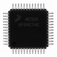
Manufacturer Part Number
MC908AP64CFAE
Description
IC MCU 64K 8MHZ SPI 48-LQFP
Manufacturer
Freescale Semiconductor
Series
HC08r
Specifications of MC908AP64CFAE
Core Processor
HC08
Core Size
8-Bit
Speed
8MHz
Connectivity
I²C, IRSCI, SCI, SPI
Peripherals
LED, LVD, POR, PWM
Number Of I /o
32
Program Memory Size
64KB (64K x 8)
Program Memory Type
FLASH
Ram Size
2K x 8
Voltage - Supply (vcc/vdd)
2.7 V ~ 5.5 V
Data Converters
A/D 8x10b
Oscillator Type
Internal
Operating Temperature
-40°C ~ 85°C
Package / Case
48-LQFP
Cpu Family
HC08
Device Core Size
8b
Frequency (max)
8MHz
Interface Type
SCI/SPI
Total Internal Ram Size
2KB
# I/os (max)
32
Number Of Timers - General Purpose
4
Operating Supply Voltage (typ)
3.3/5V
Operating Supply Voltage (max)
5.5V
Operating Supply Voltage (min)
2.7V
On-chip Adc
8-chx10-bit
Instruction Set Architecture
CISC
Operating Temp Range
-40C to 85C
Operating Temperature Classification
Industrial
Mounting
Surface Mount
Pin Count
48
Package Type
LQFP
Controller Family/series
HC08
No. Of I/o's
32
Ram Memory Size
2KB
Cpu Speed
8MHz
No. Of Timers
2
Embedded Interface Type
I2C, SCI, SPI
Rohs Compliant
Yes
Processor Series
HC08AP
Core
HC08
Data Bus Width
8 bit
Data Ram Size
2 KB
Maximum Clock Frequency
8 MHz
Number Of Programmable I/os
32
Number Of Timers
4
Maximum Operating Temperature
+ 85 C
Mounting Style
SMD/SMT
Development Tools By Supplier
FSICEBASE, DEMO908AP64E, M68CBL05CE
Minimum Operating Temperature
- 40 C
Package
48LQFP
Family Name
HC08
Maximum Speed
8 MHz
Operating Supply Voltage
3.3|5 V
Lead Free Status / RoHS Status
Lead free / RoHS Compliant
Eeprom Size
-
Lead Free Status / Rohs Status
Compliant
Available stocks
Company
Part Number
Manufacturer
Quantity
Price
Company:

Part Number:
MC908AP64CFAE
Manufacturer:
Freescale
Quantity:
3 359
Company:
Part Number:
MC908AP64CFAE
Manufacturer:
Freescale Semiconductor
Quantity:
10 000
Company:
Part Number:
MC908AP64CFAER
Manufacturer:
Freescale Semiconductor
Quantity:
10 000


6.3.9
6.4
6.4.1
6.4.2
6.4.3
6.4.4
6.4.5
6.4.6
6.4.7
6.4.8
6.5
6.5.1
6.5.2
6.5.3
6.5.4
6.5.5
6.6
6.7
6.7.1
6.7.2
6.7.3
6.8
6.8.1
6.8.2
6.8.3
7.1
7.2
7.2.1
7.2.2
7.2.3
7.3
7.3.1
7.3.2
7.3.2.1
7.3.2.2
7.3.2.3
7.3.2.4
7.3.2.5
7.3.2.6
7.4
7.4.1
7.4.2
7.4.3
7.5
Freescale Semiconductor
I/O Signals . . . . . . . . . . . . . . . . . . . . . . . . . . . . . . . . . . . . . . . . . . . . . . . . . . . . . . . . . . . . . . . . . 87
CGM Registers . . . . . . . . . . . . . . . . . . . . . . . . . . . . . . . . . . . . . . . . . . . . . . . . . . . . . . . . . . . . . 88
Interrupts . . . . . . . . . . . . . . . . . . . . . . . . . . . . . . . . . . . . . . . . . . . . . . . . . . . . . . . . . . . . . . . . . . 93
Special Modes . . . . . . . . . . . . . . . . . . . . . . . . . . . . . . . . . . . . . . . . . . . . . . . . . . . . . . . . . . . . . . 94
Acquisition/Lock Time Specifications . . . . . . . . . . . . . . . . . . . . . . . . . . . . . . . . . . . . . . . . . . . . . 95
Introduction . . . . . . . . . . . . . . . . . . . . . . . . . . . . . . . . . . . . . . . . . . . . . . . . . . . . . . . . . . . . . . . . 97
SIM Bus Clock Control and Generation . . . . . . . . . . . . . . . . . . . . . . . . . . . . . . . . . . . . . . . . . . . 99
Reset and System Initialization . . . . . . . . . . . . . . . . . . . . . . . . . . . . . . . . . . . . . . . . . . . . . . . . 100
SIM Counter . . . . . . . . . . . . . . . . . . . . . . . . . . . . . . . . . . . . . . . . . . . . . . . . . . . . . . . . . . . . . . . 103
Exception Control. . . . . . . . . . . . . . . . . . . . . . . . . . . . . . . . . . . . . . . . . . . . . . . . . . . . . . . . . . . 104
CGM External Connections . . . . . . . . . . . . . . . . . . . . . . . . . . . . . . . . . . . . . . . . . . . . . . . . . 87
External Filter Capacitor Pin (CGMXFC) . . . . . . . . . . . . . . . . . . . . . . . . . . . . . . . . . . . . . . . 87
PLL Analog Power Pin (V
PLL Analog Ground Pin (V
Oscillator Output Frequency Signal (CGMXCLK) . . . . . . . . . . . . . . . . . . . . . . . . . . . . . . . . 88
CGM Reference Clock (CGMRCLK) . . . . . . . . . . . . . . . . . . . . . . . . . . . . . . . . . . . . . . . . . . 88
CGM VCO Clock Output (CGMVCLK) . . . . . . . . . . . . . . . . . . . . . . . . . . . . . . . . . . . . . . . . . 88
CGM Base Clock Output (CGMOUT) . . . . . . . . . . . . . . . . . . . . . . . . . . . . . . . . . . . . . . . . . 88
CGM CPU Interrupt (CGMINT) . . . . . . . . . . . . . . . . . . . . . . . . . . . . . . . . . . . . . . . . . . . . . . 88
PLL Control Register . . . . . . . . . . . . . . . . . . . . . . . . . . . . . . . . . . . . . . . . . . . . . . . . . . . . . . 89
PLL Bandwidth Control Register . . . . . . . . . . . . . . . . . . . . . . . . . . . . . . . . . . . . . . . . . . . . . 91
PLL Multiplier Select Registers . . . . . . . . . . . . . . . . . . . . . . . . . . . . . . . . . . . . . . . . . . . . . . 92
PLL VCO Range Select Register . . . . . . . . . . . . . . . . . . . . . . . . . . . . . . . . . . . . . . . . . . . . . 92
PLL Reference Divider Select Register . . . . . . . . . . . . . . . . . . . . . . . . . . . . . . . . . . . . . . . . 93
Wait Mode . . . . . . . . . . . . . . . . . . . . . . . . . . . . . . . . . . . . . . . . . . . . . . . . . . . . . . . . . . . . . . 94
Stop Mode . . . . . . . . . . . . . . . . . . . . . . . . . . . . . . . . . . . . . . . . . . . . . . . . . . . . . . . . . . . . . . 94
CGM During Break Interrupts. . . . . . . . . . . . . . . . . . . . . . . . . . . . . . . . . . . . . . . . . . . . . . . . 94
Acquisition/Lock Time Definitions . . . . . . . . . . . . . . . . . . . . . . . . . . . . . . . . . . . . . . . . . . . . 95
Parametric Influences on Reaction Time . . . . . . . . . . . . . . . . . . . . . . . . . . . . . . . . . . . . . . . 95
Choosing a Filter . . . . . . . . . . . . . . . . . . . . . . . . . . . . . . . . . . . . . . . . . . . . . . . . . . . . . . . . . 96
Bus Timing . . . . . . . . . . . . . . . . . . . . . . . . . . . . . . . . . . . . . . . . . . . . . . . . . . . . . . . . . . . . . . 99
Clock Start-up from POR or LVI Reset . . . . . . . . . . . . . . . . . . . . . . . . . . . . . . . . . . . . . . . 100
Clocks in Stop Mode and Wait Mode . . . . . . . . . . . . . . . . . . . . . . . . . . . . . . . . . . . . . . . . . 100
External Pin Reset . . . . . . . . . . . . . . . . . . . . . . . . . . . . . . . . . . . . . . . . . . . . . . . . . . . . . . . 100
Active Resets from Internal Sources . . . . . . . . . . . . . . . . . . . . . . . . . . . . . . . . . . . . . . . . . 101
SIM Counter During Power-On Reset . . . . . . . . . . . . . . . . . . . . . . . . . . . . . . . . . . . . . . . . 103
SIM Counter During Stop Mode Recovery. . . . . . . . . . . . . . . . . . . . . . . . . . . . . . . . . . . . . 103
SIM Counter and Reset States . . . . . . . . . . . . . . . . . . . . . . . . . . . . . . . . . . . . . . . . . . . . . 104
Power-On Reset . . . . . . . . . . . . . . . . . . . . . . . . . . . . . . . . . . . . . . . . . . . . . . . . . . . . . . . 101
Computer Operating Properly (COP) Reset . . . . . . . . . . . . . . . . . . . . . . . . . . . . . . . . . . 102
Illegal Opcode Reset . . . . . . . . . . . . . . . . . . . . . . . . . . . . . . . . . . . . . . . . . . . . . . . . . . . 102
Illegal Address Reset . . . . . . . . . . . . . . . . . . . . . . . . . . . . . . . . . . . . . . . . . . . . . . . . . . . 103
Low-Voltage Inhibit (LVI) Reset . . . . . . . . . . . . . . . . . . . . . . . . . . . . . . . . . . . . . . . . . . . 103
Monitor Mode Entry Module Reset . . . . . . . . . . . . . . . . . . . . . . . . . . . . . . . . . . . . . . . . . 103
System Integration Module (SIM)
MC68HC908AP Family Data Sheet, Rev. 4
DDA
SSA
) . . . . . . . . . . . . . . . . . . . . . . . . . . . . . . . . . . . . . . . . . . . . . . . 87
) . . . . . . . . . . . . . . . . . . . . . . . . . . . . . . . . . . . . . . . . . . . . . . 88
Chapter 7
9
Related parts for MC908AP64CFAE
Image
Part Number
Description
Manufacturer
Datasheet
Request
R

Part Number:
Description:
Manufacturer:
Freescale Semiconductor, Inc
Datasheet:
Part Number:
Description:
Manufacturer:
Freescale Semiconductor, Inc
Datasheet:
Part Number:
Description:
Manufacturer:
Freescale Semiconductor, Inc
Datasheet:
Part Number:
Description:
Manufacturer:
Freescale Semiconductor, Inc
Datasheet:
Part Number:
Description:
Manufacturer:
Freescale Semiconductor, Inc
Datasheet:
Part Number:
Description:
Manufacturer:
Freescale Semiconductor, Inc
Datasheet:
Part Number:
Description:
Manufacturer:
Freescale Semiconductor, Inc
Datasheet:
Part Number:
Description:
Manufacturer:
Freescale Semiconductor, Inc
Datasheet:
Part Number:
Description:
Manufacturer:
Freescale Semiconductor, Inc
Datasheet:
Part Number:
Description:
Manufacturer:
Freescale Semiconductor, Inc
Datasheet:
Part Number:
Description:
Manufacturer:
Freescale Semiconductor, Inc
Datasheet:
Part Number:
Description:
Manufacturer:
Freescale Semiconductor, Inc
Datasheet:
Part Number:
Description:
Manufacturer:
Freescale Semiconductor, Inc
Datasheet:
Part Number:
Description:
Manufacturer:
Freescale Semiconductor, Inc
Datasheet:
Part Number:
Description:
Manufacturer:
Freescale Semiconductor, Inc
Datasheet: