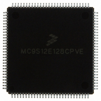
MC9S12E128CPVE Freescale Semiconductor, MC9S12E128CPVE Datasheet - Page 148

MC9S12E128CPVE
Manufacturer Part Number
MC9S12E128CPVE
Description
IC MCU 128K FLASH 25MHZ 112-LQFP
Manufacturer
Freescale Semiconductor
Series
HCS12r
Specifications of MC9S12E128CPVE
Core Processor
HCS12
Core Size
16-Bit
Speed
25MHz
Connectivity
EBI/EMI, I²C, SCI, SPI
Peripherals
POR, PWM, WDT
Number Of I /o
91
Program Memory Size
128KB (128K x 8)
Program Memory Type
FLASH
Ram Size
8K x 8
Voltage - Supply (vcc/vdd)
2.35 V ~ 2.75 V
Data Converters
A/D 16x10b; D/A 2x8b
Oscillator Type
Internal
Operating Temperature
-40°C ~ 85°C
Package / Case
112-LQFP
Processor Series
S12E
Core
HCS12
Data Bus Width
16 bit
Data Ram Size
8 KB
Interface Type
SCI/SPI
Maximum Clock Frequency
25 MHz
Number Of Programmable I/os
92
Number Of Timers
12
Operating Supply Voltage
3.135 V to 5.5 V
Maximum Operating Temperature
+ 85 C
Mounting Style
SMD/SMT
3rd Party Development Tools
EWHCS12
Minimum Operating Temperature
- 40 C
On-chip Adc
16-ch x 10-bit
On-chip Dac
2-ch x 8-bit
Controller Family/series
HCS12/S12X
No. Of I/o's
90
Ram Memory Size
8KB
Cpu Speed
25MHz
No. Of Timers
4
Embedded Interface Type
I2C, SCI, SPI
Rohs Compliant
Yes
For Use With
M68EVB912E128 - BOARD EVAL FOR MC9S12E128/64
Lead Free Status / RoHS Status
Lead free / RoHS Compliant
Eeprom Size
-
Lead Free Status / Rohs Status
Lead free / RoHS Compliant
Available stocks
Company
Part Number
Manufacturer
Quantity
Price
Company:
Part Number:
MC9S12E128CPVE
Manufacturer:
Freescale Semiconductor
Quantity:
10 000
- Current page: 148 of 606
- Download datasheet (4Mb)
Chapter 3 Port Integration Module (PIM9E128V1)
3.3.5
Port S is associated with the serial peripheral interface (SPI) and serial communication interfaces (SCI0
and SCI1). Each pin is assigned to these modules according to the following priority: SPI/SCI1/SCI0 >
general-purpose I/O.
When the SPI is enabled, the PS[7:4] pins become SS, SCK, MOSI, and MISO respectively. Refer to the
SPI block description chapter for information on enabling and disabling the SPI.
When the SCI1 receiver and transmitter are enabled, the PS[3:2] pins become TXD1 and RXD1
respectively. When the SCI0 receiver and transmitter are enabled, the PS[1:0] pins become TXD0 and
RXD0 respectively. Refer to the SCI block description chapter for information on enabling and disabling
the SCI receiver and transmitter.
During reset, port S pins are configured as high-impedance inputs.
3.3.5.1
Read: Anytime. Write: Anytime.
If the associated data direction bit (DDRSx) is set to 1 (output), a read returns the value of the I/O register
bit. If the associated data direction bit (DDRSx) is set to 0 (input), a read returns the value of the pin.
3.3.5.2
Read: Anytime. Write: Never, writes to this register have no effect.
This register always reads back the status of the associated pins.
148
SCI1/SCI0
Reset
Reset
SPI:
W
R
W
R
:
PTIS7
Port S
Port S I/O Register (PTS)
Port S Input Register (PTIS)
PTS7
u
7
SS
7
0
= Reserved or Unimplemented
PTIS6
PTS6
u
SCK
6
0
6
Figure 3-30. Port S Input Register (PTIS)
Figure 3-29. Port S I/O Register (PTS)
PTIS5
MC9S12E128 Data Sheet, Rev. 1.07
PTS5
MOSI
u
5
0
5
PTIS4
PTS4
MISO
u
4
0
4
u = Unaffected by reset
PTIS3
PTS3
TXD1
u
3
0
3
PTIS2
PTS2
RXD1
u
2
0
2
Freescale Semiconductor
PTIS1
PTS1
TXD0
u
1
0
1
PTIS0
PTS0
RXD0
u
0
0
0
Related parts for MC9S12E128CPVE
Image
Part Number
Description
Manufacturer
Datasheet
Request
R
Part Number:
Description:
Manufacturer:
Freescale Semiconductor, Inc
Datasheet:
Part Number:
Description:
Manufacturer:
Freescale Semiconductor, Inc
Datasheet:
Part Number:
Description:
Manufacturer:
Freescale Semiconductor, Inc
Datasheet:
Part Number:
Description:
Manufacturer:
Freescale Semiconductor, Inc
Datasheet:
Part Number:
Description:
Manufacturer:
Freescale Semiconductor, Inc
Datasheet:
Part Number:
Description:
Manufacturer:
Freescale Semiconductor, Inc
Datasheet:
Part Number:
Description:
Manufacturer:
Freescale Semiconductor, Inc
Datasheet:
Part Number:
Description:
Manufacturer:
Freescale Semiconductor, Inc
Datasheet:
Part Number:
Description:
Manufacturer:
Freescale Semiconductor, Inc
Datasheet:
Part Number:
Description:
Manufacturer:
Freescale Semiconductor, Inc
Datasheet:
Part Number:
Description:
Manufacturer:
Freescale Semiconductor, Inc
Datasheet:
Part Number:
Description:
Manufacturer:
Freescale Semiconductor, Inc
Datasheet:
Part Number:
Description:
Manufacturer:
Freescale Semiconductor, Inc
Datasheet:
Part Number:
Description:
Manufacturer:
Freescale Semiconductor, Inc
Datasheet:
Part Number:
Description:
Manufacturer:
Freescale Semiconductor, Inc
Datasheet:


